This thread has been locked.

If you have a related question, please click the "Ask a related question" button in the top right corner. The newly created question will be automatically linked to this question.

UCC28950: slua560c Time delay equation expalination

Part Number: UCC28950

hello

In SLUA560C in equation no 122 from where that 2.25 is coming? is it related to zvs from 50% to 100%? When refered SLUA107A it is given that 

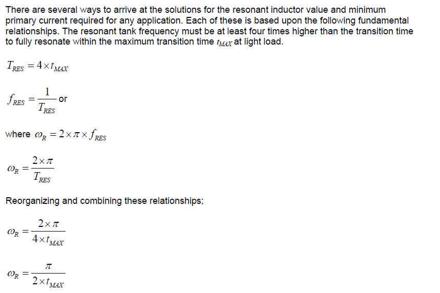
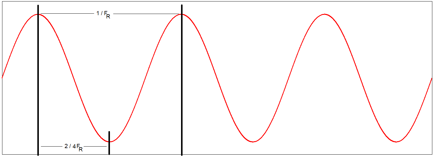
Why it is that tank frequency FOUR times higher?

and if you put last equation in terms of frequency and rearrange. it comes out that Tmax= 1/(4*fr) where fr is resonant tank frequency in Hz.
so were is that factor 2.25 is coming in equation no 122. and factor 2 in equation no 75?

please explain.

thanks

samrat

  • Hello Samrat

    The 2.25 factor in eq 122 is an empirical factor based on test data. I am not aware of any analytical derivation for it.

    I couldn't find the other text in SLUA560C, can you please recheck - maybe give me a page number for example.

    Regards
    Colin
  • Hello colin

    Factor 2 is in equation 75 on page no 13 of the SLUA560C and I am not getting why is that tank frequency should be four times the maximum transition time(this is the T_ABSET right?). That means to say minimum four oscillations of the tank are needed to achieve ZVS? Is it?
    but then that factor 2.25 or 2 makes it two or lesser oscillations insted of four. How do we justify ? what is exact relation between tank frequency and T_ABSET? T_ABSET Should be more than the time time period of tank but by what factor? on which basis?

    It is recommended to keep T_ABSET fixed and higher, what if we keep maximum possible T_ABSET (fixed), is there any other consequence apart from reduced maximum duty cyle? can we still achieve ZVS?

    thanks
    samrat
  • Thanks Samrat - I found it.

    The resonant transition must take at most one half of the resonant period of the tank circuit (Ls and C). I don't know why the equation was expressed as 2/ (4*Fr) but I think the diagram below shows that the time is actually 1/(2*Fr). The reference to the tank frequency being four times higher than the maximum transition time is misleading - the tank period should be about 4 times longer than the transition time. The reason for the resonant period being 4 times the transition time is to provide some buffer time, during which the body diode of the MOSFET is conducting, to allow for variations in the IC and transition timing. If you haven't turned the MOSFET on by 1/ (2*FR) the resonance will continue and the MOSFET drain voltage will increase again and you lose ZVS.

    Regards

    Colin 

  • hello colin

    "tank period should should be four times longer the transition time?" are you sure?
    then the whole document SLUA107A is in ambiguity ?

    let us just get it cleared..!

    with ZVS we can remove only turn on losses? RIGHT? Suppose TOP switch is on and when we turn off that switch the resonance will start with frequency of fR. So you mean to say if we dont turn on the bottom switch before the (1/2fR) Time we will not have ZVS.

    Then also you mean to say ..if we keep delay time more than (1/2fR). We will never have ZVS? IF I GO FOR ZVS...SHOOT THROUGH IS WAITING..!!!!!!! IS IT?

    THANKS
    samrat
  • Hello Samrat

    Yes, I'm afraid that SLUA107A is a bit ambiguous in this regard.

    The resonant period will start when the top switch is turned OFF and will ring with a frequency of fR. The RATE at which it charges the capacitance at the switched node will depend on the current in the inductance at the moment the switch is turned OFF so the TIME needed for the node to be charged from Vin to 0V (at which time the body diode of the low MOSFET turns on) will be shorter at higher currents. If the current is too low there may not be enough energy to charge the node all the way to zero and you will not achieve ZVS. Note though that even if you charge only 50% of the way down and then turn the LOW side MOSFET on you will incurr only 25% of the switching losses that you would if you hard switched all the way from Vin to 0V.
    Now, assume that there is enough energy (current) in the inductor to ring the node down to 0V - this current will then flow in the body diode. The current will reduce at a rate di/dt = V/L where V is the input voltage (during this time the full input voltage appears across the leakage inductance (shim inductor). Eventually the current will reverse and the body diode will turn off. The switched node is then unclamped and will ring up again. The trick is to turn the low side MOSFET on before this happens.
    The same argument applies for both positive and negative going transistions - note that the Left hand leg (QA/QB) transition is different to the Right hand leg transition - this is explained in http://www.ti.com/lit/slup102 , http://www.ti.com/lit/slup101

    You are right, if you wait too long to turn the MOSFET ON you will lose ZVS because the node will ring up again, if you don't wait long enough you will turn it ON before the node rings down fully again losing ZVS.

    Normally a controller like the UCC28950 will prevent the shoot through condition where both FETs are on at the same time but if you have asymmetrical propagation delays in the two channels the control signals might become skewed enough to cause shoot through. These propagation delays aren't within TIs control - the designer has to take care.

    Regards
    Colin
  • hello colin
    thanks for the references.
    Samrat.