This thread has been locked.

If you have a related question, please click the "Ask a related question" button in the top right corner. The newly created question will be automatically linked to this question.

UCC27524A: ucc27524 failures rate

Part Number: UCC27524A
Other Parts Discussed in Thread: TIDA-00779, , UCC27524, UCC27531

Dear TI Team,

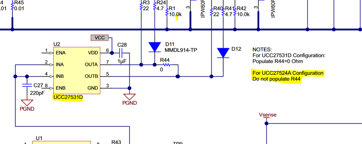
            We are developing TIDA-00779 as per reference design. In this MOSFET driver section we are using ucc27524a instead of ucc27531D.

And tested upto 2A Load but in this ucc27524A got short on Vcc to Gnd very often and failed 10 Nos . Kindly suggest best fit circuit for ucc27524.

Ganesh


  • Hi Ganesh,

    Thanks for your interest with TIDA-00779 and UCC27524A. I am an apps engineer with this device and will help you solve this issue.
    You are using the 524A to drive 2 parallel lowside FETs in this PFC boost TIDA and the 524A experiences a VDD-GND short just about every time a 2A load is applied.

    What Key System Parameters are changed from TIDA-00779 (Table1)?
    How long does it take for the failure to occur after applying the load? Is there any other pin besides VDD that’s damaged for instance OUTA/B?

    There are a number of ways a VDD-GND short could occur. The first thing to do is to verify the voltage on VDD during the short failure. VDD abs max is 20V, its possible that any voltage over this voltage for any period of time could damage the part. what is the VDD voltage during the time of failure?

    Can you share your schematic so I can do a review? If the schematic review tells us nothing nothing then to find out whats causing this we may need to test out on the bench and observe some scopeshots. There could be negative voltage reflected from GND, poor VCC regulation, OUTA/B might exceed ratings, power dissipation is too high, etc.

    Thanks,
  • Hi Jeff,
    Thanks for you immediate response, We are working on as per TIDA-00779, No Key system parameters not changed in table 1.
    also This will not fail when it is in loading and it will fails during switching on PFC and if PWM outA/B disabled that time also it fails.here with attached the schematic for your perusal suggest your ideas.
  • Hi Ganesh,

    Thanks for your update and schematic. This schematic from TIDA-00779 mention two configurations for two different drivers, one is the UCC27531 and the UCC27524A. The Figure below highlights this.

    The pinout shown is actually the pinout for the UCC27531 which is the single split output driver in which R44 (same as R120 on your schematic) would be needed to sink current. In the case of using the UCC27524A you would not populate R44 since there is a driver channel for each power MOSFET. Since you have R44 populated, some of the turn OFF current is making its way to VDD and not to GND damaging the device.

    Please let me know if this answers your question!

    Thanks,

  • Dear Jeffery,

           Actually  In our prototype board we didn't populate the R44.(As per your Instruction)

    everything, we are testing based on your TIDA-00779.

    Thanks 

    Ganesh

  • Hi Ganesh,

    Thanks for the update. Do you know what is the VDD voltage during the time of failure?

    Can you share scopeshots of VDD and both outputs during the time of the failure?

    Thanks,

  • Hi Ganesh,

    just wanted to see if there is any progress with this issue?

    Thanks,
  • HI Jeffery,
    This is the wave form we captured during switching on PFC system, But the failures occurred during ideal condition when auxiliary power supply switched on.
    1. the IC got during the load whenever we cross load more than 2-4A, Sometimes During switching On PFC and some times when it is in ideal condition.

    Thanks & Regards
    Ganesamurthy.S
  • Hi Ganesh,

    Thanks for your update, to confirm the scope shot, this is of VDD? and where is GND located on this scopeshot or can you confirm how high VDD reaches?

    also, the aux supply your referring to is the 5V supply connected to J12 or the 12V supply connected to J8?

    I noticed that TIDA-00779 needs an external bias supply to power the gate driver (among other things). You are generating this 12V external bias in the 'power section' of your schematic with a flyback topology. If the scopeshot is from VDD then could it be possible that this 12V flyback supply is experiencing too much flyback exceeding the 20V abs max rating?

    I see there is also a clamp at the pri/sec to limit the voltage spike caused by the leakage inductance. A lower value for the clamping resistor, Rclamp=R146 can be used to discharge Cclamp, R92, quicker by dissipating the stored leakage bringing the node back to the initial switching state. Similarly, series resistor R148 for example can be reduced so that Cclamp can better handle the high peak currents during turn-off. Likewise, C90 on the secondary can be increased to limit the voltage rise while still absorbing the leakage.

    Thanks, 

  • Hi Jeff,

                 Thanks for your support, after experimenting your suggestions i will come back with results.

    and there is no doubt on 12V supply to ucc27524, we are applying only 12V not 5V.

    Thanks 

    Ganesh.S