This thread has been locked.

If you have a related question, please click the "Ask a related question" button in the top right corner. The newly created question will be automatically linked to this question.

TPS65218: Can I Connect L5 \FB5 \ L6\ FB6 to ground?

Part Number: TPS65218

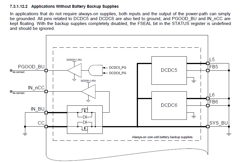
If I don' t need to use TPS65218' DCDC5 and DCDC6 channel , can I just connect  L5 \FB5 \ L6\ FB6 to ground?

  • DO NOT tie all these pins to GND.

    You must leave L5 and L6 floating (NC, or not connected) if the DCDC5/6 converters will never be used so not current can flow through this path.

    FB5 and FB6 should be pulled up to a voltage higher than the expected output voltage (VDCDC5 > 1.0V, VDCDC6 > 1.8V) so that the feedback loop never tries to engage the FETs.

    You can pull these up to VIN or DCDC4 through a 10kOhm resistor.

    If you want to try to remove these resistors later, you can test the design by removing them and measuring quiescent current. If the current increaes with FB5 and FB6 floating, then they will need to be assembled in the final design.

  • The reason for tying VFB higher than the output voltage is because there is only a VPG monitor on these converters. The voltage must be over the expected output for the PGOOD_BU signal to become active.

    If PGOOD_BU will not be used, it is theoretically okay to tie FB5 and FB6 to GND.

    For all other DCDC1-4 converters, they affect the primary PGOOD and have VPG and VOV thresholds, so an output inductor (at Lx pin) and capacitor (to hold a charge) are mandatory in order to maintain a regulated output voltage for the FBx pin to read a correct value and for PGOOD to be active.
  • Hi, Brain:

    Here is a screenshot form datasheet:

    It seems we can tie these 4 pins to GND on condition that IN_BU and CC also tied to GND.

    While,I want to use SYS_BU this time. So I can not tie IN_BU to GND.

  • Yes, your understanding is 100% correct.

    If the entire sub-system is not used, all of the pins can be tied to GND (IN_BU, SYS_BU, CC, L5, FB5, L6, FB6, PG_GOOD_BU, IN_nCC) without any issues.

    If input power is applied at IN_BU to provide output power at SYS_BU as you have described, then L5 and L6 cannot be tied to GND.
  • Hi, Brian:

    I will leave L5 and L6 floating, pull FB5 and FB6 up to VIN.

    Now, I have another question:

    Yesterday, I powered the CC pin with a DC voltage of 3V, but the DCDC5 and DCDC6 channel don' t work. When I decrease the input voltage to 2.6, these two channel works.

    While the datasheet shows:

    It seems 2.2V to 3.3V will all be OK.