This thread has been locked.

If you have a related question, please click the "Ask a related question" button in the top right corner. The newly created question will be automatically linked to this question.

LM27762: The negative output doesn't reach the designed value. Positive works fine

Part Number: LM27762

Hi everybody, newbe here.

I recently design a board for the LM27762, my aim is to have a dual rail supply for some op amps. Let's say +- 5 V @250 mA.

The main issue is that I can't get the right negative voltage from the IC. The positive output works fine.

PCB schema

PCB layout

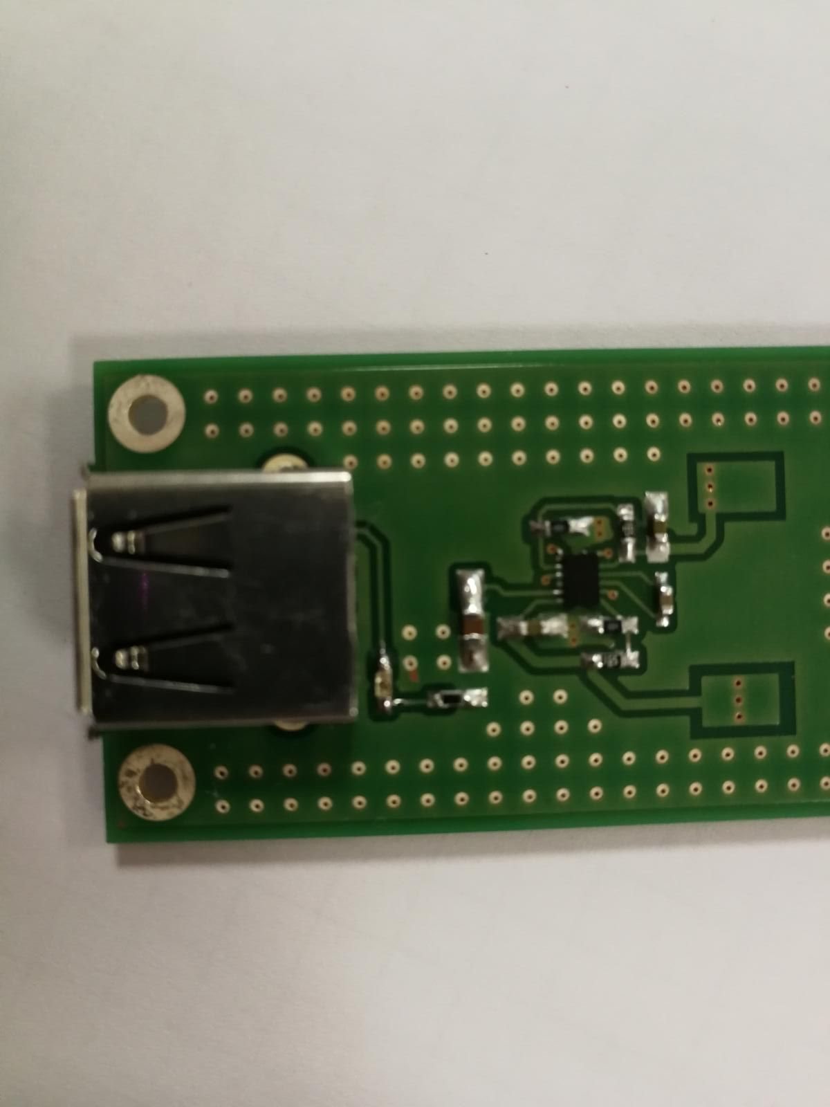
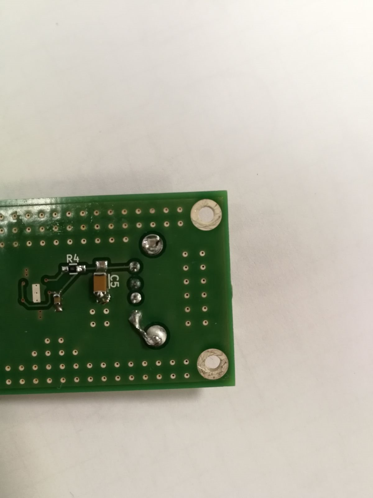
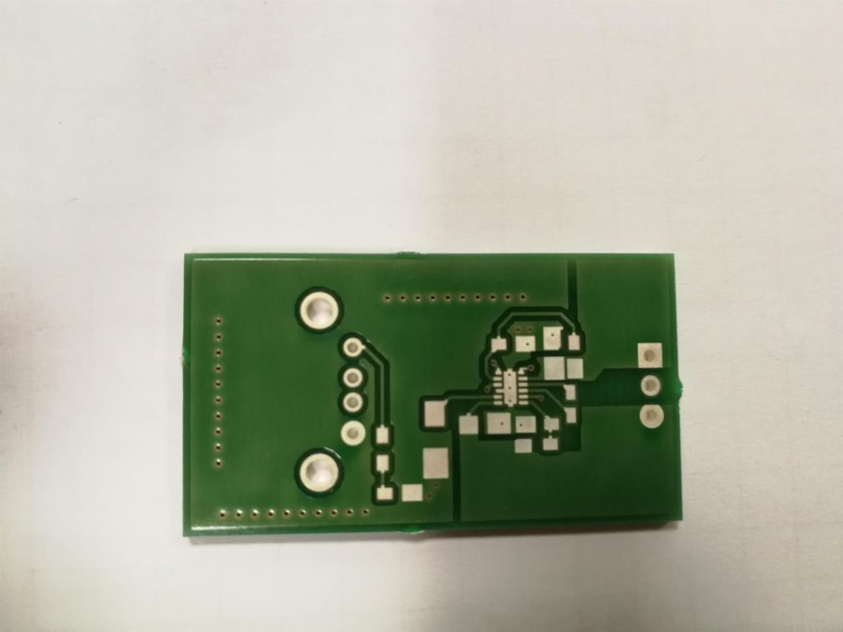
photo

Front                                                                                                           Back


BOM

R3 - 1.5k P1.50KHCT-ND

LED -APTD1608LCGCK

C5 - 10uF GRM31CR61H106MA12L

R4 -10k  CRCW060310K0FKTA

C16- 1uF 732-7907-1-ND

C19-4.7uF C2012X5R1E475K125AB

R5/R14  1.6M YAG3327CT-ND

R12/R13 500k RC1608F4993CS

C17/C18 2.2uF 311-1814-1-ND

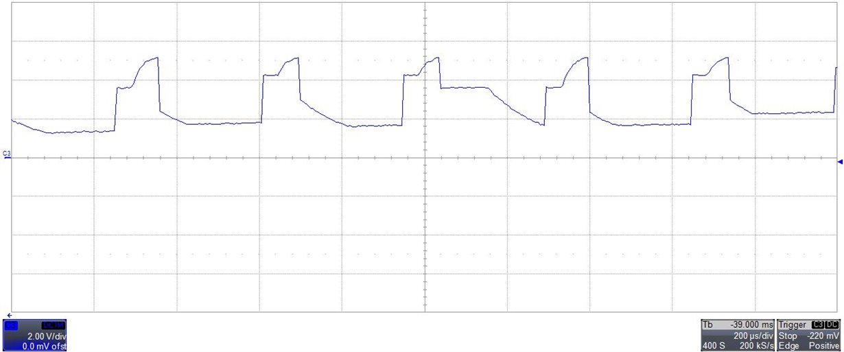
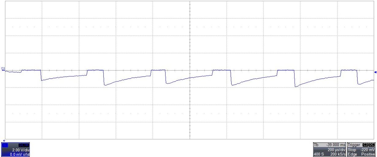
Oscilloscope output:

Positive and negative output:

Positive and negative zoom

C+ and C-

What I did wrong? Thank you in advance.

  • Alessandro,

    Thank you for giving so much information to work with. A couple of questions/recommendations from my end.

    1. Does this issue happen only when you connect the device to the op-amp or is it happening on its own?
    2. Is the EN- pin connected to Vin? It looks like it is not on the layout, but it looks like it is in the board picture.
    3. What is the input voltage looking like?
    4. Try using a 10uF cap for CP. The datasheet recommends it for higher currents.
    5. In general some of you traces could be bigger for things like your input voltage. You can look at the EVM layout to see a good example.

    Please let me know if any of this helps or if you have any other questions.

    Thank you,
    Nick
  • Hi NIck, thanks a ton for helping me.

    I will answer point by point:

    1. The load of the circuit is the 1M ohm DC coupled channel of my LeCroy oscilloscope. The measurement is done with a simple osscilloscope probe 1X.

    2. Yes you are right, I posted  the wrong pcb layout. The EN- pad is connected.

    This is the correct PCB layout 

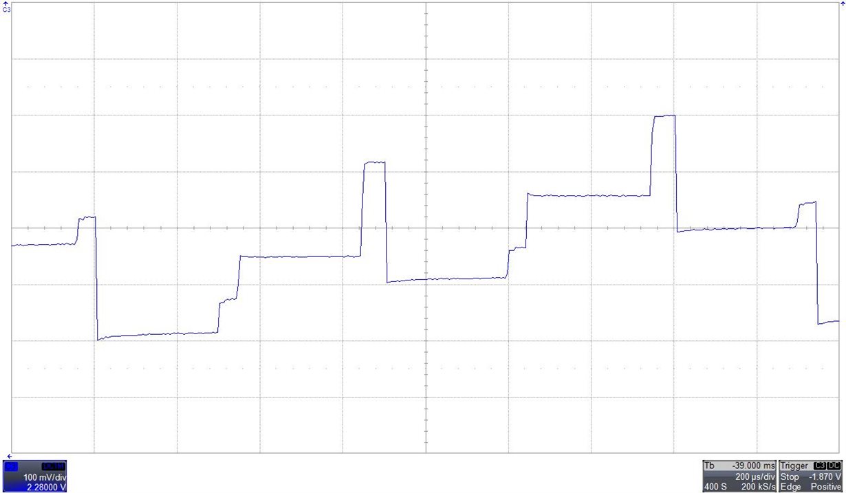
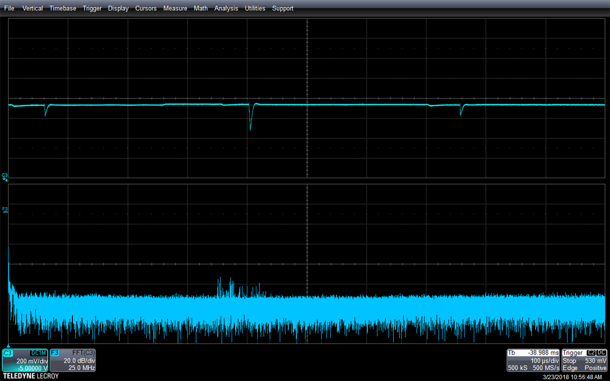
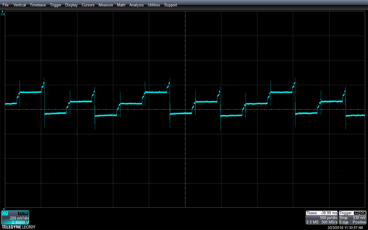
    This is the signal on EN- pin

    This is the zoom on the same signal

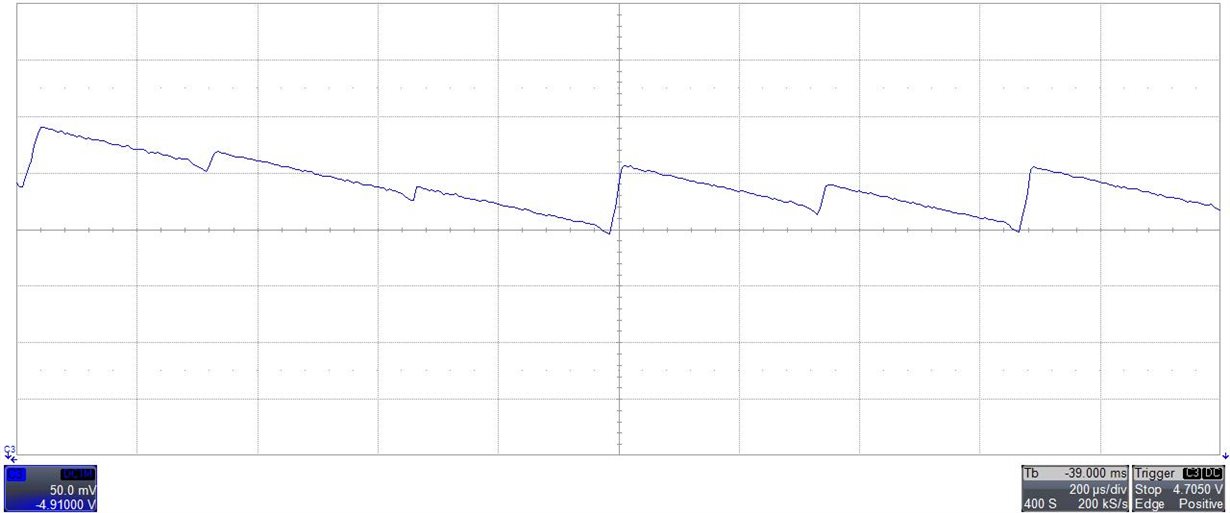
    3. This is the signal of Vin

    4. I changed the CP as you suggested 

    Vout + works fine

    Vout - locked on around -2V 

    5. Regarding this point unfortunately I can not print a new board with larger traces, but I have an other PCB to test, where the layout is similar to the EVM board.

    Do you any other suggestion? I evaluated that 0.250 A the limit trace width should be 0.1mm 

    Thank you very much for your support :)

  • Hi Alessandro,

    Instead of making your own PCB, can you order the EVM and test it? This is why we provide them :)

    On both of your layouts, it looks like the input cap is on the back of the PCB. Adding any space in this connection adds inductance which is not desired.

    Are you able to show Vin, CP, and OUT- on the scope at once?

    Finally, are you powering this from a USB cable or 5V lab supply? I recommend using a known 5V power source in this first round of debugging.