This thread has been locked.

If you have a related question, please click the "Ask a related question" button in the top right corner. The newly created question will be automatically linked to this question.

UCC27714: HO outputs stay on high - EN disabled via pull down

Guru 55913 points
Part Number: UCC27714
Other Parts Discussed in Thread: TIDA-00778

Hello,

Condition reported few weeks ago was thought to be leakage of HB since no FET's were yet installed. Sadly reported condition remains after they were installed both HO/LO gate drive.

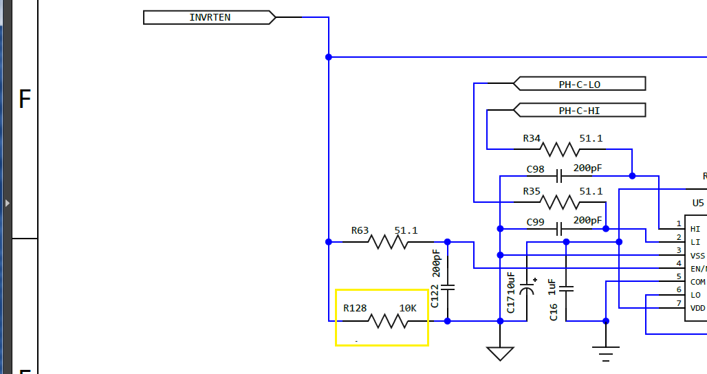
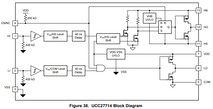
POR of MCU PWM pins 1/2 (pull down 20k) and GPIO drive EN pin 4 to three UC devices have EN line pulled down 10k is 0V when HO goes high.

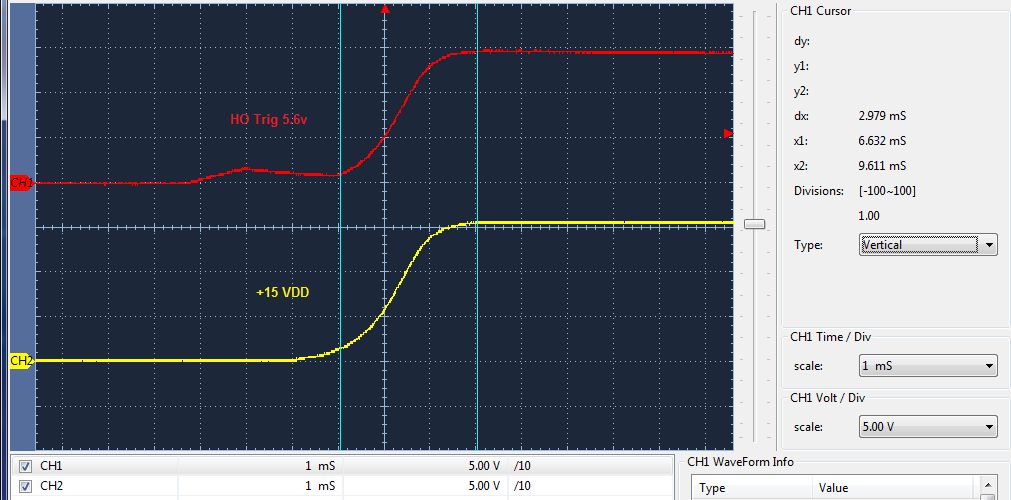
Power supply +15 VDD has 2.97ms delay up to 80% of 3v3 MCU power capture posted below. These UC have been setting HO high on POR and do not follow truth tables in datasheet. Made sure to solder iron temp 258*C for less than 10 seconds per pin most were done in less than 4 seconds, solder to pads look very clean not cold. Have 20k/16v zener in parallel across HS/HO pins 11/12 and measure +13v on either pin.

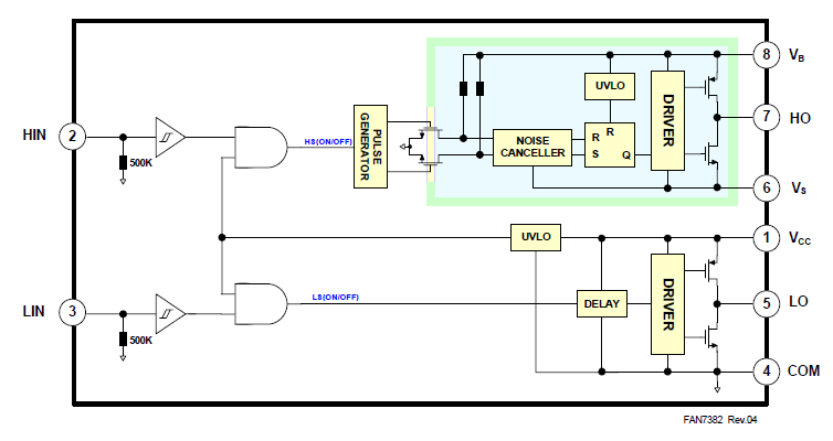
What is causing the HO to stay on all the time, seems LO is keeping 0v during POR. Any PWM drive to pins 1/2 cause 1/2 bridge shoot through with MCU Panic shut down. 

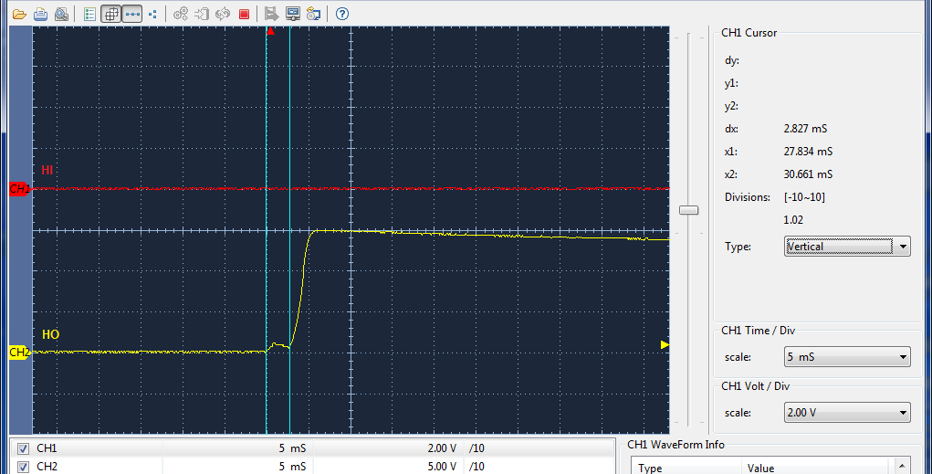
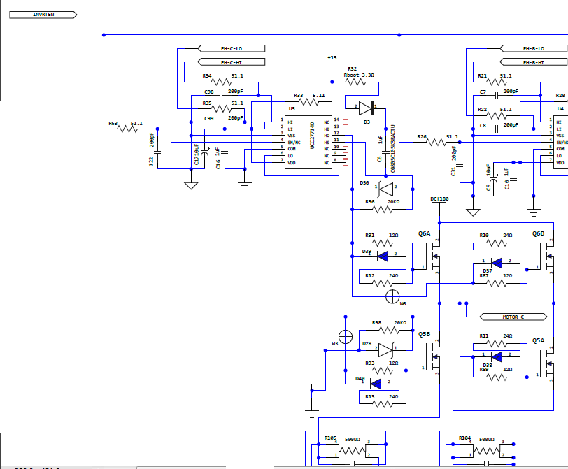
Applied power to system: HO to VDD rise:

  • Hello BP101,

    Thanks for your interest in UCC27714 as well as the additional information and captures. We will be sure to help you get to the bottom of this.

    To get this straight, the MCU goes through POR and the EN input is pulled to 0V. The MCU powers up, followed by VDD ~3ms later. HO comes on at the same time as VDD, even with EN pulled low. It then stays high and causes shoot through when the low side is turned on. Does that sound like what you're seeing?

    Curious about the little amount of voltage on HO before VDD rise. Is there any voltage on your power stage when performing this testing? Do you have any shots of enable and HI pins when power is applied to the system? Also, could you please share the part of the schematic relating to the driver? This would help get a better understanding of the system, especially since it seems to happen to all three devices.

    Best Regards,

    John
  • Hi John, Thanks for quick reply!

    John Geiger said:
    To get this straight, the MCU goes through POR and the EN input is pulled to 0V

    No the EN pin is static low prior to POR and then GPIO enabled with weak pull down but 0v measured on pin 4 after POR.

    John Geiger said:
    Curious about the little amount of voltage on HO before VDD rise. Is there any voltage on your power stage when performing this testing? Do

    Yes the same 20v DC supply that is also used to buck +15v for VDD rise shown second capture CH2.

    John Geiger said:
    Do you have any shots of enable and HI pins when power is applied to the system? A

    Nothing happen on HI to trigger scope (trig 0-180mv) yet HO goes high like below capture. The HO capture above is actually the gate leg of FET rising just above ground (POR) roughly 1.2v then shooting up to rail on all 3 gate drivers. question remains how can all 3 gate drivers defeat the truth table in datasheet. Have double checked there are no shorts between DC buss supply or HO drives or HB/HS pins. Odd thing is the High side HO outputs without any FETS installed was doing the very same thing whether EN was controlled by GPIO or not. Now EN it is GPIO controlled & 10k pulled low as described above. 

    Perhaps we have bad batch of chips here?

  • BP101 said:
    Odd thing is the High side HO outputs without any FETS installed was doing the very same thing whether EN was controlled by GPIO or not

    What I mean to say is after seeing the EN buss from 3v3 GPIO rise to 4.4v prior to flashing MCU, immediately disconnected all EN pins by removing 51.1 ohm series resistors. That was prior to installing the FETS and according to TM4C1294 datasheet the GPIO pins are high impedance state prior to flashing the firmware.

    The EN pins were disconnected from the MCU control, yet the HO outputs measured +12.6vdc. The internal 200k pull up on EN limits current to 75uA VDD 15v, hard to imagine MCU caused damage to UC enable pin especially since it was never flashed. Only recently added a 10k pull down on EN buss upon installing FETS and three new 51ohm, returning EN pin 4 to MCU GPIO control.

    So when I say static10k pull down that is not to say the EN pin could be rising up 1.92v when GPIO output driving EN pins enters POR high impedance but that seems unlikely to cause HO to bonce high.

    Might it be disastrous if the EN pin has any truth allowing HO's to jump to rail? Seems unlikely since with EN disconnected from MCU the HO's still jump to VDD rail on scope and drops to roughly 13.3v.

  • Schematic of EN drive:

  • Hi BP101,

    Thank you for all the information. It seems you've adequately ruled out voltage on EN and HI causing the glitch. One thing that doesn't seem right is the fact that the bootstrap capacitor can charge at all. Normally, the bootstrap cap only charges when the low side is switched on, shorting the switch node to ground and providing a path for current from HB to GND. The high side output then uses this charged capacitor to switch the high side FET with Vcb+Vin. If LO is successfully staying off on POR, there should be no current path for charging Cbs.

    Your scope shots show HO immediately following VDD, which means there is a current path to charge the bootstrap cap.

    Can you do a couple measurements of resistance and forward voltage as follows?
    VDD-HB
    HB-VDD
    HB-HO
    HO-HB
    HO-HS
    HS-HO
    HS-GND
    GND-HS

    Also, with the setup running steady-state, could you measure the voltage drops across Rboot and D3? This could give us a good idea of how much current is going from VDD-HB, and might be the reason HO drops to 13.3V as you observed.

    Best Regards,
    John
  • John Geiger said:
    Your scope shots show HO immediately following VDD, which means there is a current path to charge the bootstrap cap.

    Actually the scope is triggering CH1/HO and it starts to rise before VDD but then quickly dives down before shooting up, so much for single channel captures.

    I checked the Dboot diodes 1uf ceramic caps are installed correctly have 15vdc as schematic shows. The HO outputs were reading 12.6v prior to FETS being installed, reason to ask about the external zener being place directly across pin 11/12 versus after the gate resistor. Recalling Tina produced odd transient analysis around zener diode on gate drive. Tina support forum then asked to start analysis with zero values, seemed to stop HO output going high without HI being present. What say you to that?

    There was no ESD during install (wrist straps 50% RH 68*F) but the chips were shipped without black anti static foam. Reading in data sheet foam is required were shipped by Arrow in anti-static bag with moister seal dates, chips installed same day open moisture bag with blue dots on card. 

  • John Geiger said:
    Normally, the bootstrap cap only charges when the low side is switched on, shorting the switch node to ground and providing a path for current from HB to GND.

    Why do you guys always think the +13.3v across HO/HS is leaking through Rboot/Dboot and not originating internally through the ESD protection diodes? Tina was showing HI was high on start of analysis, not HO imagined recall, start transient analysis with initial values stopped Hi (high) causing a low on HO. So the zener was causing high voltage on HO in similar analysis tests, with zero initial conditions.

    There is no excessive current draw via VDD as the +15 buck IC remains ice cold. Again have to consider the transition of EN pin (1.92v float) during MCU POR may be hi jacking the OVP circuit in odd way or destroyed it? The 5vdc buck and 15v buck share an RC delay to both bucks EN rise to 2.9v supply which causes a delay of LDO 3v3.

    If a 59uA current draw destroyed the EN pin circuit of tree UCC tied together then these UC need to have a silicon design review ASAP!

  • BTW:

    John I can PM the entire schematic for review and it should be reviewed by Derek too since this behavior of HO is dam odd. This is not my first rodeo with similar gate drivers in a 3 phase 1/2 bridge configuration but never had HO go high like this. Will check unpopulated PCB too which passed US board house electrical testing, thus being certified!
  • Blank PCB rings out ok as expected no issues per schematic nor prototype with other vendors gate drivers same basic inverter circuit, no EN drives. The problem seems to be the RS latch inside UCC27714 is not clearing HO side drives no matter how EN is handled on POR, e.g. EN low (0v)then 2 second delay switch EN high (3.2v) or start with EN high (3.2v), 2 second delay switch EN low (0v) or leave EN floating on POR same issue HO goes high all gate drivers. There was always some leakage into low side DS through high side DS of FETS but HO was never being turned on either side during POR, that causes shoot through and blown fuses FETS etc...

    Sure seems some kind of VDD errata, what is trick to stop it from occurring? The 16v zener across UCC pins 11-12 being removed did not stop HO shooting high.

    The EN pins on all UCC via diode check measure 0.740v(COM)/1.34v(VDD) drop, e.g. NO ESD rail diodes shorted. HS/HO to COM 170k++. HB to COM 1.6--megohms. VDD to GND 8.7k. The ohms (++) increase or (--) decrease charging 680uf cap on high side FET drains.
  • Hi BP101,

    Can you remove the 180V bus voltage, temporarily short HS to GND with a jumper wire or something, and check if HO still shoots high?

    Regards,

  • Hi Derek,

    Gate voltage slowly rises then goes to ground when jumper is grounded. The HS pin is directly to each motor phase between high side source and low side drain. There is no load connected to the bridge at this time.
  • Leakage current into Cboot from ground can not effect HO operation according to the datasheet, good thing that or ADC phase FB monitors would be useless. Seemingly the internal RS latch driver should be holding HO in the off state when VDD is of steady state. Have ordered 6 UCC from TI store today.  Perhaps accidently touching DMM probe from VDD onto INVRTEN (51R1) caused some kind of internal issue with RS latching HO? Really hard to imagine that (200k pull up, EN input) such a thing occurring but that nasty probe did short GPIO pin rail diode, yet the MCU would still write flash and run applications. That MCU was replaced twice for USB port failures which has noting to do with EN pins of the three UCC gate drivers.

    MCU POR:

    The UCC27714 includes protection features wherein the outputs are held low when inputs are floating or when the minimum input pulse width specification is not met. The driver inputs are CMOS and TTL compatible for easy interface to digital power controllers and analog controllers alike. An optional enable and disable function is included in Pin 4 of the UCC27714. The pin is internally pulled to VDD for active-high logic and can be left open (NC) for standard operation when outputs are enable by default. If the pin is pulled to GND, then outputs are disabled.

    7.3.1 VDD and Under Voltage Lockout

    The UCC27714 has an internal under voltage-lockout (UVLO) protection feature on the supply circuit blocks between VDD and VSS pins, as well as between HB and HS pins. When VDD bias voltage is lower than the VVDD(on) threshold at device start-up or lower than VVDD(off) after start-up, the VDD UVLO feature holds both the LO and HO outputs LOW, regardless of the status of the HI and LI inputs. On the other hand, if HB-HS bias supply voltage is lower than the VVHB(on) threshold at start-up or VVHB(off) after start-up, the HB-HS UVLO feature only holds HO to LOW, regardless of the status of the HI. The LO output status is not affected by the HB-HS UVLO feature (see Table 1 and Table 2). This allows the LO output to turn-on and re-charge the HB-HS capacitor using the boot-strap circuit and thus allows HB-HS bias voltage to surpass the VVHB(on) threshold.

  • Hi BP101,

    Can you measure the HO to HS voltage when HS is left floating, then measure again when it is grounded? HO is pulled to HS when disabled or turned off, so there should be 0V between the two, even if they both measure high to GND with HS left floating.

    Best Regards,

    John

  • Hi John,

    I already clarified that in Derek's replay that HO slowly rises along with HS to 12.6v and HO drops at 0v when HS is pulled to ground. 

    That would actually be disastrous if BEMF could continue to trigger HO and not actually turn HO off when PWM drive stops. Are you sure about that as other industry gate drivers do not behave like that. When HO is off HO is off no matter what HS or HB are doing. That's kind of the point behind PWM driving the FET/IGBT device connected to HO and not some other outside conditions be able to influence HO causing shoot through in the bridge.

    Could it be you mean when EN is low then HO is pulled to HS and then again that would not actually disable HO if HS can continue to effect HO.  Seemingly that would be an engineering design flaw of the IC's HO drive architecture.

    HO must be disconnected from any driving source when it is disabled (high impedance) or PWM drive is low HO remains OFF. Otherwise you too have discovered what I am reporting in several posts and a trouble ticket needs to be opened so we can get this silicon corrected ASAP!

  • Hi BP101,

    From your description, it sounds like the part is working normally. HO must be measured with respect to HS in all scenarios. Since HS is connected to the source of the high-side MOSFET, both the UVLO condition and the disable condition effectively short the gate of the MOSFET to the source through the gate drive resistance, clamping it in the off-state. Independent of the HS voltage, the gate-source voltage should still be held at 0V.

    If instead the outputs were to transition to high-impedance during these conditions, there is a possibility that leakage currents, transients, or changes in the gate-drain to gate-source capacitance ratio due to the application of the high voltage bus could trap charge on the gate capacitance and turn on the high-side MOSFET unexpectedly. A resistor from gate to source helps to alleviate this problem, at the cost of higher operating current whenever the outputs go high. Clamping the output low (HO to HS, LO to COM) during disable or UVLO behaves similarly to this clamp resistor, just with much lower resistance.

    HO and HS both rise to about 12.6V in response to the 15V supply starting up, since they are initially connected to the 15V supply through a low-impedance bootstrap diode. Quiescent current flows into HB and out of HS, but HS is not connected to GND except capacitively. Since there is no load and no low-impedance path to GND for the quiescent current of the high side circuitry, charge will accumulate on the HS node until the HS-GND capacitance is charged high enough that the high side supply no longer draws quiescent current, or until that quiescent current is small enough that it matches the leakage current from HS to GND.

    Regards,

  • Enable is not reacting as the datasheet states enable function should and there is a ground path connected on HS, yet HO should not be driven High when HI is low in any condition not just when EN is low. Perhaps TIDA-00778 engineer designed around this HS EN defect by increasing the FB circuit ground resistance above 1 megohm. The HO outputs are not low and defeat the datasheet signals (Fig.42) and statement yellow below. If the enable is not disconnecting HO output from the FET gate motor EMF can turn the gate back on and drive a shoot through scenario. That said some how the HO output is not being controlled by the EN/HI pins as 7.4.1 also states it should be. In your scenario if the HO clamps to HS when EN is low the potential for high voltage electrocution exists to any customer that comes in contact with a switch leg believing the driven is disabled and being in emergency stop conditions.  If HS can defeat EN or HI control signals that is not proper design for any chip.

    Have to believe the EN signal has lost control of the HI/HO signals via RS latch.

    7.4.1 Enable Function

    The enable function is an extremely beneficial feature in applications where the DC-to-DC controller is located on the secondary side, which is very common with digital controllers. In these applications, it is easy to turn off the driver signal in a very short time when critical faults such as primary-side overcurrent occurs. The Enable Function response time is typically around 80 ns, refer to Figure 31, Figure 32 and Figure 45.The enable pin controls both the high-side and low-side driver-channel operation. The enable pin is based on a non-inverting configuration (active-high operation). Thus, when EN pin is driven high the driver is enabled and when EN pin is driven low the driver outputs are low. The EN pin is internally pulled up to VDD using 200-kΩ, pull-up resistor as a result of which the outputs of the device are enabled in the default state. The EN pin is left floating or Not Connected (N/C) for standard operation, where the enable feature is not needed. Care must be taken not to connect the EN pin to ground, which permanently disables the device. Like the input pins, the enable pin is also based on a TTL and CMOS compatible input-threshold logic that is independent of the supply voltage and is effectively controlled using logic signal from 3.3-V and 5-V microcontrollers. The UCC27714 also features tight control of the enable-function-threshold voltage levels which eases system design considerations and ensures stable operation across temperature (refer to Figure 20 and Figure 21).

  • HS is connected to ground 520k in our controller and in TIDA-00778 by monitoring phase FB voltages via ADC channels. We don't mind 15v on HS but do mind HO staying high when EN has disabled HO or HI is low! So it would seem if HO is high when EN is low with HI being low it can not (properly) PWM the high side FET as HO is always high when HI is low.

  • BTW: The reason for 10k or 20k resistors between the NFET gate and source is to turn off gate drive if gate signal is lost such as if HO enters the high impedance state. So clamping HS to HO is not explicitly necessary and somehow in this case keeping HO at 13v on all three UCC drivers.
  • BP101,

    If the HO voltage is equal to the HS voltage, the high side driver output is low. HO cannot go lower than one diode drop below HS for any prolonged duration, because the output body diode between HO and HS would clamp HO to HS within one diode drop. This is explicitly stated in the absolute maximum ratings table. This will always be true, even if the output could be toggled to high impedance.

    If the HO voltage is greater than the HS voltage by a substantial amount, while the EN signal is low, I agree this is a problem. Otherwise, the driver is functioning normally. The only time that HO is high is when the HO voltage is equal to the HB voltage, and the HB voltage is greater than the HS voltage. It sounds like you are measuring that the HO voltage is equal to the HS voltage when EN is low. This is normal, intended behavior.

    Regards,
  • Derek Payne said:
    The only time that HO is high is when the HO voltage is equal to the HB voltage, and the HB voltage is greater than the HS voltage

    How about when the HI is low and EN is low HO should too be low not high like it returns too after a PWM pulse. That is working the NFET gate backwards.

    Derek Payne said:
    It sounds like you are measuring that the HO voltage is equal to the HS voltage when EN is low. This is normal, intended behavior.

    And that would cause 1/2 bridge immediate shoot through like it does when other vendors gate drivers never kept HO high after producing a PWM pulse. Both HO Totem pole drivers should be in the OFF state when RS latch Q output turns off the switch pair (together). Never separately like you are suggesting HS somehow latches to HO in the disabled state, how does that follow truth table 7.3.2? HO returning high after producing a PWM pulse also violates truth table 7.3.2 if EN is Low. So something ain't right here.

    We would rather see this issue be our mistake than TI making a design error then pandering everything works ok when our case simply does not add up to being even close to ok, relative to truth table 7.3.2.

    Below is the gate driver TI used in previous LMi RDK we adopted some time ago and have tested TM4C1294 MCU works effectively to drive the inverter stage prior to recently updating to UCC27714 drivers. Clearly everyone is following similar Table 7.3.2 truth rules for 1/2 bride drive designs. These 3 UCC gate drivers recently installed violate the truth table several different ways and do not keep HO low, when EN is kept low HI is kept low HO then stays high, again a very dangerous concept no body in the industry should ever support. The emergency PWM shut down algorithm immediately disables EN if current on any of the 1/2 bridges exceed the trip level current of 11.4 amps. That emergency condition is also explicitly stated in the datasheet to disable HO output and the NFETS are on their own life support at that point, not the gate drivers.

  • BP101,

    Are you referring to this block diagram, where the output of the RS latch is using Q instead of Q'? I believe this is an error that must be corrected in the image.

    Regards,

  • Derek Payne said:
    Are you referring to this block diagram, where the output of the RS latch is using Q instead of Q'? I believe this is an error that must be corrected in the image

    The upper PFET seems to never switch off as Q toggles low or high even when EN is made low or high, HI is being ignored and HO never changes (static) state of HI . Such simple logic behavior violates truth table 7.3.2.

    The truth table 7.3.2 is either correct or IC is defective, no in between!  Especially since Fig54 capture can not be produced statically by toggling EN pin to either state and HO remains high. The only time HO changes state is on the falling edge of HI after it first rises, that is inverted HO operation relative to HI input logic.

    The part that makes no since is accidently touching DMM probe across 15VDD into the EN pin buss (INVRTEN) may somehow have destroyed R input structure of all 3 gate drivers RS latch. Can you verify if doing such destroys the R part of the RS latch, datasheet AMR shows EN pin input @17V Max? Would it not behoove TI to design counter measures into the RS latch to stop undesired current flow as described above if it indeed exists? 

  • Hi John,

    Voltage measurements of HS to HO being (0v) with EN low does seem to suggest HO being clamped to HS, but not from a ground perspective. Suppose this issue also has something to do with how HO voltage reaches VDD where other vendors gate driver HO keep below VDD from a ground reference when HI is kept low.

    Must admit my idea of what disabled via EN meant, HO would be high impedance where safety resistor (10k-20k) NFET gate to source was the only life boat to keep destructive faulted NFET gate back current from burning the HO output drive in a crash.
  • Hello BP101,

    Yes, as explained previously by Derek, HO clamping to HS is the intended behavior of this device, and is the "LOW" state. Since the source of the high side FET is referenced to HS, this behavior means the high side Vgs is kept at 0V - which means the FET is turned off and does not conduct. HO does not connect to ground in order to retain isolation between HS and GND - especially with high voltage on HS. HO should be measured in reference to HS for this type of circuit.

    Best Regards,

    John
  • Perhaps specifying that HO truth table is relative to HS would help remove any further questions of table 7.3.2 be qualified to the EN logic input level.

    It would seem from results of low NFET shunt monitor a significant current surge occurs as disabled HO voltage transitions from a floating level up to full VDD rail and above.

    That single pulse surge seems to occur only on EN being made low on the very first HO output pulse, perhaps during 20% crossing HO to LO on each 1/2 bridge. That part is very difficult to know exactly but the HO pulse falling edge does jot (-1.5v below VDD start threshold of HO relative HS being scope probed via COM ground.

    Hence the repeated question can EN pin withstand single current of 293ma when subjected to +15 VDD input that also made puff of smoke 5.1 ohm VDD pin 7 source resistor as 15v shorted the MCU GPIO rail diode to ground. I calculate the current through 3 parallel EN pin 4 each 51.1 ohm to be 17ohms or 15v/17 = 882ma. Yet it seems the new MCU GPIO is driving the EN pins without any issue that I know of.

  • Hi BP101,

    The EN pin is a high impedance input, capable of operating up to an abs. max of 20V, as specified in the data sheet section 6.1. It should not see that high of current as long as this abs. max voltage is not violated.

    Best Regards,

    John
  • I discovered software bug had HI/LI drives reversed on 3rd UCC killing the FOC closed loop though it would close loop FOC without NFETS installed. Hence being very confused what was happening to HO drives.

    One other thing not being expressed in datasheet text, when EN is disabled are HI/LI then disabled too?
  • Hi BP101,

    That's good to hear that you found the bug.

    HI/LI are inputs to the device - control of the inputs is on the controller/MCU side. EN pin controls whether the device outputs (HO/LO) can respond to HI/LI inputs. With EN disabled, the outputs HO/LO are LOW regardless of inputs HI/LI. HI/LI inputs are pulled to VSS through 400k internal resistor if left floating.

    Best Regards,

    John Geiger