This thread has been locked.

If you have a related question, please click the "Ask a related question" button in the top right corner. The newly created question will be automatically linked to this question.

LMR62421: Design reliability

Part Number: LMR62421

Hi,

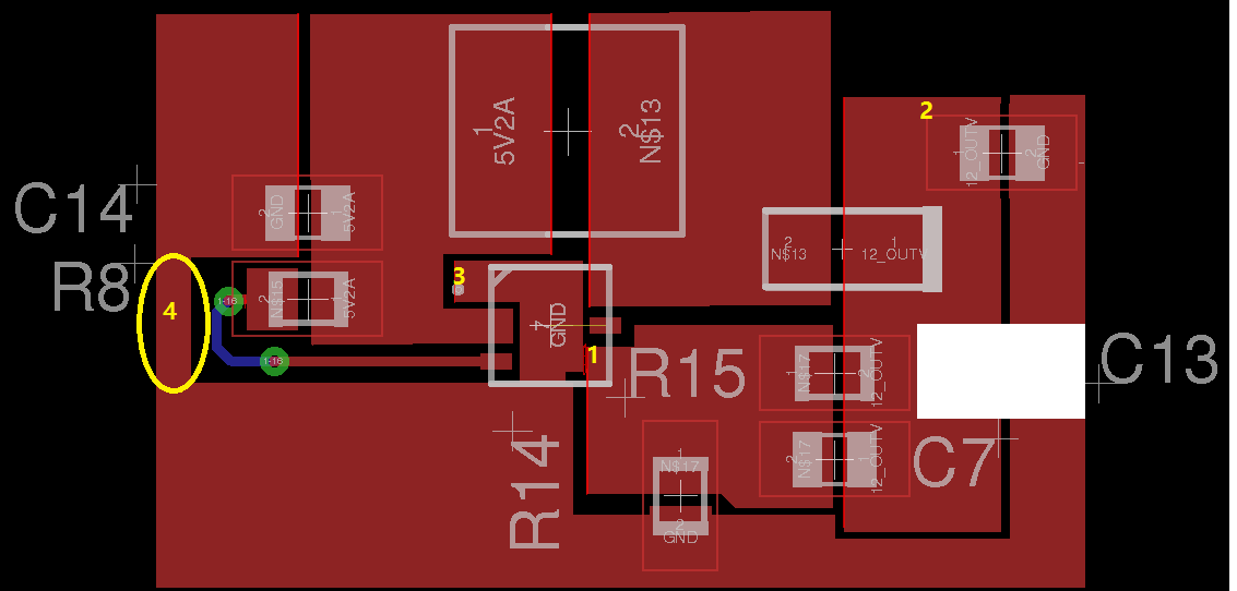
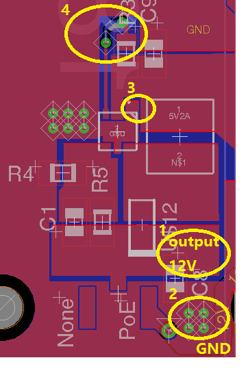
Yesterday I posted here in order to check if my boost converter layout should be suitable for the application and it didn't and for this reason, could someone could also check my 5V to 12V @ 0.5A dc dc converter using LMR62421X layout?

Thanks a lot,

Simone

  • The engineer supporting this part is currently out of office, and you will get the reply early next week. Also, could you post a cleaner layout pictures? The labels overlaps and make it hard to identify which is which on the right side of the picture.
  • Thank you for the answer.

    Sorry for the not clean layout picture. I hope this would be cleaner.

    Thanks a lot

  • Hi Simone.

    Sorry for the delay.

    There are some comments for the layout.

    1 you should connect pin5 (AGND) to thermal pad.

    2 change C13 (output cap) close to output port.

    3 Do you have two layers? If it is, it is helpful to put some vies near pin1 (PGND)

    4 If you don’t have two layers, the cupper(I highlight) is not enough.


      Thanks

      Jing

  • Dear Jing,

    Thanks a lot for the answer.

    I attached to this post the new design, integrated inside the main board I'm developing. Is this design more suitable? The pads near the out capacitor are a switch that,  when the switch is turned on,  shorts the OUT plane to the 12V trace.

    Thank you so much,

    Simone

  • Hi Simone

      It looks better. and I still have some suggestion and question.

    1 2 I have highlighted the output port and GND. I didn't get your point about "The pads near the out capacitor are a switch that,  when the switch is turned on,  shorts the OUT plane to the 12V trace."

    3 if you could put a via next GND pin, it will be better. because the will be a current flow in GND pin.

    4 I am just curious why you use two vias to connect R3 to EN, I think you could connect it directly in top layer.

    Thanks

    Jing

  • Hi Jing,

    I removed the vias as you mentioned in 4 and added one as you mentioned in 3. Regarding the first 2 points, the pads named "None" and "Poe" will be connected to the central one in order to decide or not to enable the 12V line using something like this

    to make te contact.

    Attached to this post is my final design.

    Thanks a lot for the help

    Simone