This thread has been locked.

If you have a related question, please click the "Ask a related question" button in the top right corner. The newly created question will be automatically linked to this question.

UCC27211: IC getting extremely hot and smoking

Part Number: UCC27211
Other Parts Discussed in Thread: UCC20520

Hello,

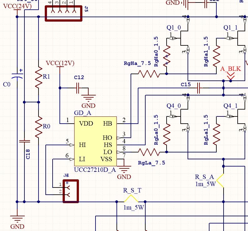
We have been working on making a 3 phase BLDC motor controller with switching implemented through UCC27211 High/Low driver. To start with, we began testing each of the phases of the designed motor controller at no load (nothing connected to the phase outputs). Here is a part of the schematic for reference:

However, after a while IC starts drawing tremendous amount of current (up to 0.4 Amps) through VDD at 12V supply, DC Link at 6V, gets tremendously hot, starts smoking and eventually fails.

Here are some of the scope snapshots for reference:

a. A_BLK - GND

b. HB-HS(Across Cboot)

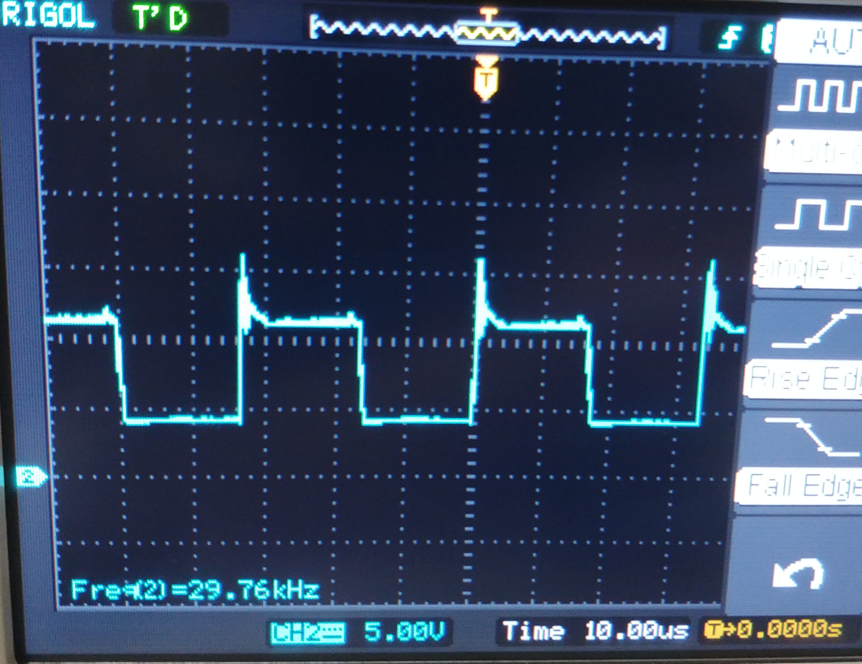
c. High Side - Channel 1; Low Side - Channel 2

The gate resistances used are 7.5 ohm common for both MOSFET with 1.5 ohm additionally for each parallel MOSFET

Any immediate help towards solving this issue would be highly appreciated. :)

  • Hi Manuj,

    Welcome to e2e, and thanks for your interest in our devices.

    I don't see anything obviously wrong on your schematic.

    However, the HS-HB oscilloscope plot looks different than I would assume. It should go to ground when the low-side FET turns on, but you seem to have a 5V offset. I wonder if that's the problem? I'd recommend investigating that area first.

    Let us know what you find, and we can help with other suggestions if that's not it.
  • Hi Manuj,

    thanks for your post Don and Manuj! thanks for reaching out Manuj and being my friend on e2e:)

    Don spotted something interesting. The bootstrap voltage has a very large ripple. HB-HS voltage should be relatively constant so it can efficiently turn on/off the floating highside fet without having too large peak bootstrap charging currents (for example during start up when HB-HS is much less than VDD).

    There is evidence of the bootstrap not getting enough charge - seen from the last scope shot HO appears to be less than 10V which can drive the fet toward the linear region creating even more heat.

    can you tell me what your Cboot and Cvdd as well as what fet you are using?
    Generally, Cvdd=10*Cboot=10*Cgate

    Thanks,
  • Hi Jeff,

    Thanks for your reply.

    We are using the following FET (IRF1018E): www.infineon.com/.../irf1018epbf.pdf

    It has 8mohm (Rds) at Vgs = 10V and Qgs of approximately 70nC each; we have two MOSFETs in parallel making Qgs to total of 140nC. Please let us know what do you infer by Cgate.

    Also, we are using 100nF Cboot (16V rating) with same value for Cvdd also.  We are confused with the waveform across Cboot, the voltage drops to around 5V but we still can see in the last scope shot the voltage at HO is around 8-9V. We are not able to see any relation between voltages across Cboot and HO-HS. However we also found the following waveforms for the Vgs of the MOSFETS:

    We are not really sure about the exact moment of its capture, we found it randomly during the testing. We are really burning through our IC before we could do any thorough testing. However if you notice, the Vgs for channel 1 here is approximately 5v which is same as the Cboot voltage in corresponding part of its cycle as in the image posted in the question. Now, if we go by this captured waveform, we are left with two issues; i.e. high current drain in IC and its burning and Vgs often not going up to 12 Volts.

    Please suggest next steps to us in process of debugging the issue.

    Thanks and Regards

    Manuj Agrawal


  • Hi Manuj,

    Thanks for the update. Since your Cboot and Cvdd are the same value then when the time comes for Cboot to be replenished (and Cvdd is charged to VDD) then the maximum final setting voltage that Cboot can possibly replenish to equals half of VDD. Ic*dt/(Cboot+Cvdd)=dV.

    If we set Cvdd to be 10*Cboot or at least 1uF then the ripple on Cboot should also reduce by a factor of 10.

    Can you test out this value for Cvdd and update me with the results?

    Thanks, 

  • Hi Jeff,

    Thanks for the response. I will update you as soon as we get more ICs delivered to us. In the mean time, please let us know how can the ripple on Cboot lead to large current draw and high temperatures. Can it be due to high value of dv/dt across it? We have been testing with very low value of DC link voltage, = 6 volts, and no load on any of the phases.

    Thanks and Regards
    Manuj

  • Hi Don,

    We think that HS-HB should go to Vdd when the low-side FET is on, please confirm.
  • Hi Manuj,

    The energy stored in Cboot during one period of the ripple; W_ripple = Cboot*dVcboot^2 = ~10uJ
    however the sufficient charge/energy for the HS fet; Qboot > = Cgate*dVgs where W_Qboot = Qboot * dVgs = ~840nJ

    W_Qboot << W_ripple therefore the power dissipated in the bootstrap charge path is dominated by dVcboot^2

    Since power consumption and gate charge are temperature and voltage dependent, the device carrying a higher current will heat up more. Total charge coming from the bootstrap Qtot = Vripple*Cboot and the larger the ripple, the more charge that’s dissipated as heat after sufficient gate charge has be supplied. Bootstrap ripple is primarily determined by the sizing of the bootstrap capacitor. The bigger the Cboot the smaller the ripple.
    Please let me know if this is not clear or you have any more questions.

    Thanks,
  • Hi Jeff,

    We are really enjoying this insightful conversation with you and appreciate your help. :)

    From your last reply we are clear about why the device is getting heated up. We are now changing our Cboot to 1uF and Cvdd to 10uF. But from your last to last reply, we are still not clear about why Cvdd should be 10*Cboot. Can you please explain it with more detail? It would be really helpful if you could relate it to the waveforms we are getting.

    Thanks,

    Manuj

  • Hi Manuj,

    Thanks for the follow up, glad to spark some conversation. I think correcting this cap value is the first step with finding a solution.

    Cboot should be 22nF-100nF. VDD cap should be 220nF-4700nF. This can be found from the UCC27211 datasheet Pin Functions seen below.

    We typically recommend a larger capacitance for VDD, 10x as a general guideline, so the current sourced from VDD to charge the bootstrap capacitor does not result in large VDD ripple. Using a guideline of the 10x for the VDD capacitance results in 1uF for VDD capacitance. It is good practice to have a lower value ceramic which has lower impedance at high frequency in parallel, so a parallel 100nF is recommended with larger VDD capacitance values.

    On a system perspective, ripple on HB means large boot diode currents to forward and reverse bias it due to a larger potential difference on this diode. For instance, if the HS turns on and there is still current charging the BS from LS being on then the BS will experience a greater loss due to reverse recovery which permanent damage might occur. Another example would be If there is very low LS on time and/or a boot cap that is much larger than required, that can also cause this issue.

    Does this make sense?

    Thanks,

  • Hi Jeff,

    We understand that with larger ripple at HB, the boost diode will face greater reverse recovery losses. The last paragraph you mentioned is very clear. We are also clear about why we require a larger Cvdd.

    We have another doubt which we feel is very crucial. Suppose we want to keep the ripple on Cboot to 0.5V and the gate charge required to turn ON FET is 140nC(Possible in case if we use parallel FETs), the size of Cboot required would be 280nF (Cboot = Charge required by gate to turn ON FET / delta V). But it is stated in the datasheet that Cboot is generally within 100nF, does this mean we should look another FET driver which can support providing such large Gate charge or we can still use this driver for the above mentioned application?

    We are considering using a 1uF cap for Cboot to include a safety margin and a 10uF, do you think this is OK? This is in reference with what we read in the datasheet of UCC20520. You can see it in the snapshot below:

  • Hi Manuj,

    Thanks for your questions/concerns as they are very understandable. UCC20520 features an external bootstrap diode and allows for an optional series resistance in the bootstrap charging path to limit losses. UCC27211 internal bootstrap diode is not suited for higher bootstrap values due to excessive power dissipation inside the device. The UCC20520 acknowledges this possible outcome at the end of the section 9.2.2.6.2 seen in the pic below. Which basically says: during startup for example, a bigger Cboot will take longer to charge and experience more loss. To combat this, a 100nF Cboot is recommended for transient performance. However this only applies to UCC20520 example in the datasheet because the boot diode is external and a boot resistor is used. There is also the difference of the power train voltage that HB rides on being 800V and heavily influencing reverse recovery.


    The AC ripple on HB is dependent on leakage (negligible) @ ~1.2mA for UCC27211 when discharging and Qtot when charging. However a DC voltage drop less then VDD on HB exists across Rboot because of large bootstrap charging currents keeping it there. A larger Rboot limits bootstrap current enough to add a larger Cboot to reduce ripple further however means a larger DC drop from VDD seen on HB. Therefore with a larger Cboot, the BS ripple will be reduced at the expense of a larger drop on Rboot and a larger Rboot would be needed for larger Cboot.

    I recommend we stick with the value limits from the datasheet as to not stress the internal boot diode.

    Thanks,