This thread has been locked.

If you have a related question, please click the "Ask a related question" button in the top right corner. The newly created question will be automatically linked to this question.

LM73605: Layout recommendation

Part Number: LM73605

Hello,

I have a new colleague (with a lot of experience in power supply designs as he said) and he don't want to use the reference layout of the datasheet, because he believes that his layout is much better.

Here is his recommended layout:


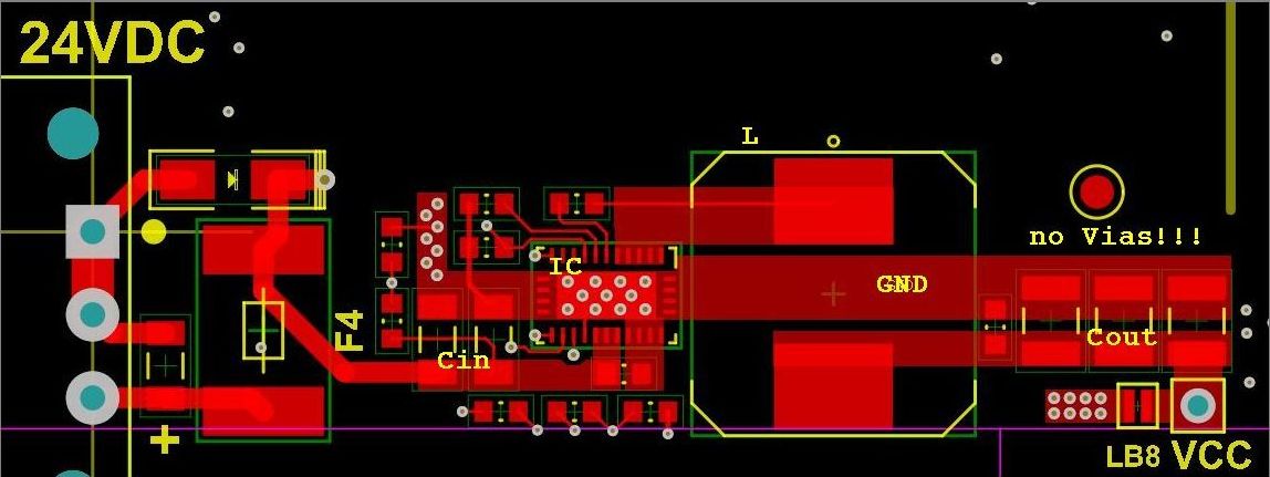
What is your opinion? What is good? What is bad?

Best regards

Alfred

  • The layout could work. My suggestion is the FB divider should be placed closer to the FB pin. One concern is that there is not much copper on the top layer to distribute heat generated on the IC. Inductor will heat up as well and the ground trace going through the inductor wouldn't help much in heat dissipation. The other side of the copper extension from the DAP is not much either.

    Use more thermal vias on the ground copper should help. Bottom layer where these thermal vias connected to should be a solid piece of copper as much as possible.

    -Yang