This thread has been locked.

If you have a related question, please click the "Ask a related question" button in the top right corner. The newly created question will be automatically linked to this question.

LMR16006: Large output ripple, well below the switching frequency

Part Number: LMR16006

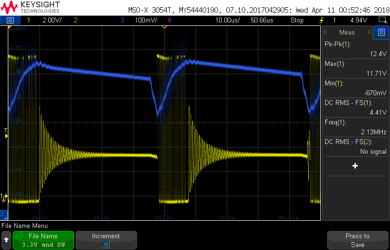
I am using a LMR16006Y (2.1MHz) to power a 3.3VDC 50mA load from a 34V - 46V DC input. I am seeing complex ripple that is about 600mV peak to peak whose frequency (20k-30kHz) is well below the switching frequency. If I zoom in I can see the switching ripple riding on this waveform at 2.1MHz and a duty cycle of ~14%, so I don't think this is being caused by the switching ripple. I'm afraid the volatility in my power source will cause EMC issues in my product when I go for compliance testing.

This oscillograph was taken under a normal load and shows the ripple I am seeing.

The following oscillograph show what the ripple does if I add an additional load of 100mA (32 ohm resistor) to the output. I did this to rule out the supply running in DCM (Discontinuous Mode). Based off of the waveform change, I think I was in DCM and am redesigning the converter accordingly. However the ripple is still way to much, so I believe these is an additional issue.

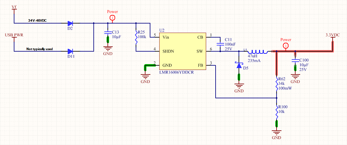
Below is the schematic for the SMPS. I have tried swapping L1 for the more appropriately sized 100µH inductor, but this has not affected the output at all.

Any help on this would be greatly appreciated.

  • Hello,
    You schematic in principle looks OK.
    However with Vin=34V and Vout=3.3V, this device will not operate at 2.1MHz switching frequency.
    If you look at the device datasheet you will notice that Tonmin=80ns typ.
    For conversion ratio above, on time would be ~50ns for Vin=34 and just ~ 35ns for operation at Vin=46V. Clearly in both cases much lower than device can actually deliver.
    If your input voltage condition are defined as stated above, one approach would be to use LMR16006X device (operating at 700kHz), and check system performance. There are not many devices that can deliver this output voltage while operating at 2.1MHz.

    In summary either device switching frequency will need to be adjusted in order to accommodate for this conversion ratio, or if operation at 2.1MHz is must input voltage could be reduced, so minimum on time limitation is not violated.
    Regards
    Brani
  • Huh... You're absolutely right. We definitely overlooked that little gem. I scoped the switch node and it is definitely switching with 80nS pulses before turning off. When it gets low enough it starts up again. It seems to stop when it hits the OVTP (Over voltage transient protection) trip point.

    I manually injected less voltage to see if this would resolve my issue and got this waveform. Yellow is the switch node (SW) and is 2V/div, blue is the 3.3VDC output rail and is 0.1V/div. During the upward slope you can see the switching waveform pumping current into the inductor, but then it stops and it looks like the diode is ringing as the inductor current falls to zero. The capacitor carries the load until some mystery event occurs, causing a large output voltage drop which forces the regulator to start pumping current into the inductor again.

  • Hello,
    From your screenshot it looks like device is hitting over voltage condition and at that moment switch node is turned off.
    When output voltage falls below certain threshold, switch node turns on and starts delivering energy into inductor.
    It also shows significant amount of ringing on the switch node.
    This could be caused by measurement method (long ground loop when using standard tip and barrel probe), or by less then optimal layout.
    Also it is not visible what type of diode are you using in your design.
    It is recommended to use diode with current rating above maximum device current rating.

    As far as overshoot on output is concerned, this type of behavior is observed when feedback voltage (for whatever reason) is not stable. So please check connections for feedback resistors and FB pin on the device. And for FB stability layout is very important. Feedback node should be routed away form noisy switch node, in order to minimize potential noise coupling into sensitive analog circuitry.
    It would be helpful to review your application layout, to verify that there are no issues with layout.

    regards
    Brani
  • Hello,
    Since there is no activity on this post, i will close it.
    Regards
    Brani