Hi everyone !
I have a question about LM25117 Data Sheet.
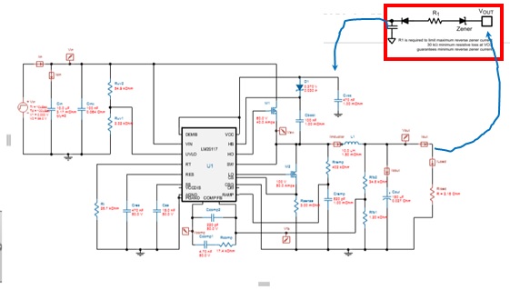
"Figure 18. External VCC Supply For 14.5 V <V OUT"
The circuit input to VCC is posted from VOUT, via Zener Diode.
-Q1: Is the circuit of Figure 18. necessary? (must applying the circuit ?)
(In the WEBENCH simulation result, the circuit of Figure 18 was not applied.)
-Q2: What are the advantages of applying the circuit in Figure 18.?
-Q3: Using the circuit in Figure 18,
I think it will collide with the VCC output terminal (internal LDO: 7.6 V typ.),
Should I disable the internal LDO on the VCCDIS pin?
- Q4: Can you suggest a recommended circuit for me?
My design specification:
Device: LM25117
Vin: 36 V
Vout: 24 V
Iout: 11 A
Please let me know if you have any information.
Best Regards
ShingLM25117.pdf