A related question is a question created from another question. When the related question is created, it will be automatically linked to the original question.
If you have a related question, please click the "Ask a related question" button in the top right corner. The newly created question will be automatically linked to this question.
Hello Taemin,
Thank you for your interest in the LM5109B-Q1. I am an application engineer supporting this device and will answer your questions on the design.
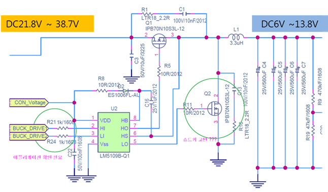
For the selection of C16, bootstrap capacitor, and C22 VDD capacitor I would suggest re-evaluation. The value of C16 is based on the gate charge of the MOSFET, operating frequency and max duty cycle. There needs to be enough charge on C16 to charge the MOSFET gate and sustain the HB voltage during the maximum on time. The IPB70N10S3L is a 60nC (80nC Max) gate charge device. This is an effective gate capacitance of 6nF to 8nF charged to 10V.
Refer to the LM5109B-Q1 datasheet www.ti.com/.../lm5109b-q1.pdf
section 8.2.2.
The value of 1uF is much larger than you will likely need, unless the switching frequency is low. 100-220nF is a more appropriate value for most power supply applications.
The bootstrap capacitor that is too large can cause issues charging the capacitor to full charge on the initial LO output pulse.
The series boot resistor, R8, of 10 Ohms is OK if the boot capacitor can be reduced.
The C22 VDD capacitor is typically recommended to be 10x the value of the bootstrap capacitor C16, so if C16 100nF is OK C22 should be 1uF.
Driver LI and HI inputs: It would be good practice to add placeholder capacitor locations for LI and HI to ground in case there is induced noise or ringing on the driver inputs. To reduce the possibility of induced noise on the LI and HI inputs, we recommend series resistance with the the driver inputs in the 10 to 100 Ohm range.
Mosfet selection: Without knowing the operating frequency and load current, TI cannot give detailed advice on these devices. Keep in mind with the MOSFET selection and 1A driver capability, the Vgs rise and fall times are estimate to be ~60ns. This may not be acceptable for very high frequency operation. If the design is high frequency, either a higher strength gate driver or lower charge MOSFETs should be considered to reduce switching losses.
The advice I provided on the previous post still applies, regarding the sizing of the bootstrap capacitor, VDD capacitor, and Mosfet & driver selection depending on operating at high frequency.
One additional recommendation, as good design practice, will be to add some resistance from the gate to source of the MOSFETs to address any leakage current from drain to source during power up of the control and driver bias.
Can you confirm on the thread if this addresses your questions?


