This thread has been locked.

If you have a related question, please click the "Ask a related question" button in the top right corner. The newly created question will be automatically linked to this question.

TPS54386: TPS54386 EMC problems - 50 MHz harmonic

Part Number: TPS54386

Dear Texas team,


This is the continuation from this post: https://e2e.ti.com/support/power_management/non-isolated_dcdc/f/196/p/645543/2381672#2381672 which is locked but not solved yet. Unfortunately Argentina official agent in charge of making EMC test is hiper slow :( so we have not any probe that the problem is truly solved.

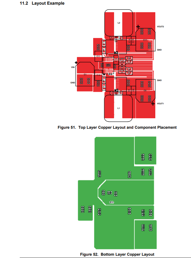
We are desingning a new revision of the PCB with the Anthony suggestions but now we have a doubt. Texas layout example for TPS has not ground plane on the bottom layer under the inductors and of course our desing is based on this example. We want to know if it's really harmful to put it because it would block the EMC in that direction.


Hope you can help us.

Best regards,


Bruno

  • Bruno,

    I am not sure why there is no dedicated GND plane on a four layer board.  I generally do not rout anything under the inductor on the top side.  However I typically will have at least one internal or bottom layer as a dedicated GND plane, including under the inductor.  If I am doing a 2 sided pcb and absolutely have to run some signal lines on the back side, I still flood the rest of the layer with GND.

  • Dear John,

    Thank you for your answer.

    In this case I have a 2 layers pcb with the exactly same layout as Texas gave in the datasheet of the TPS54386, and there is no GND on bottom layer. You can check the original post I mention with the captures of the schematic and layout of my PCB and Anthony's tips.

    I don't have any signal under the inductor, the problem is we have a radiated harmonic on 50 MHz which is over the maximum permitted.

    As I understand from your experience there is no problem to flood the bottom layer with GND plane, right?

    Best regards,

    Bruno
  • Bruno,

    While it does not explicitly say so in the datasheet, It appears that the entire back side consists of four copper areas; Vout1, Vout2, a central "quiet ground" for connection to the thermal pad and an outer generally "C" shaped circulating current return GND. I would have no issue extending that circulating current return under the two inductors. I would leave the two grounds separated as shown.
  • Dear John,

    You mean something like this, right?


    Best regards,

    Bruno

  • Bruno,

    Yes exactly.