This thread has been locked.

If you have a related question, please click the "Ask a related question" button in the top right corner. The newly created question will be automatically linked to this question.

TPS56C215: Boards reset when using 2 separate grounds.

Expert 2415 points
Part Number: TPS56C215

Hi Ti,

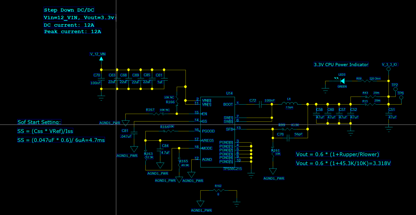
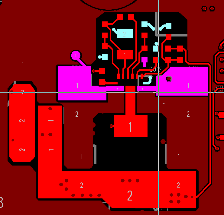
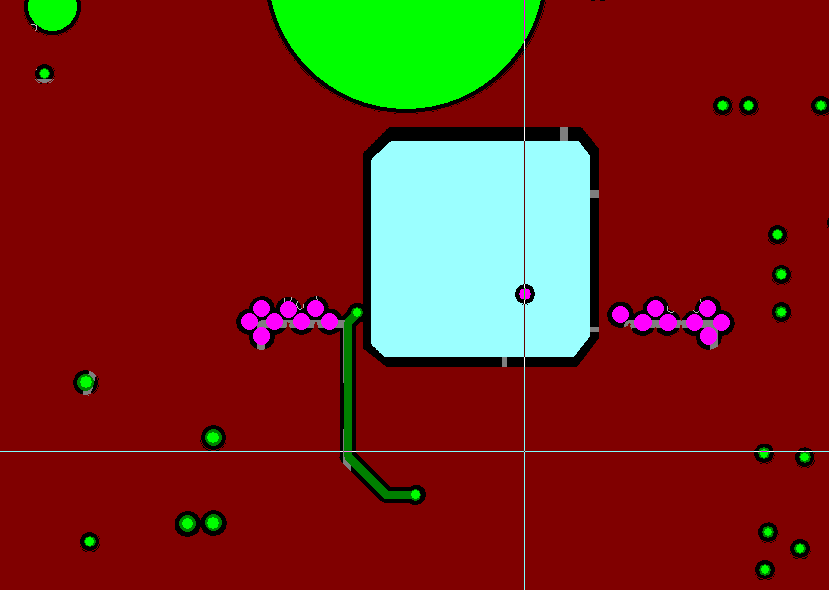
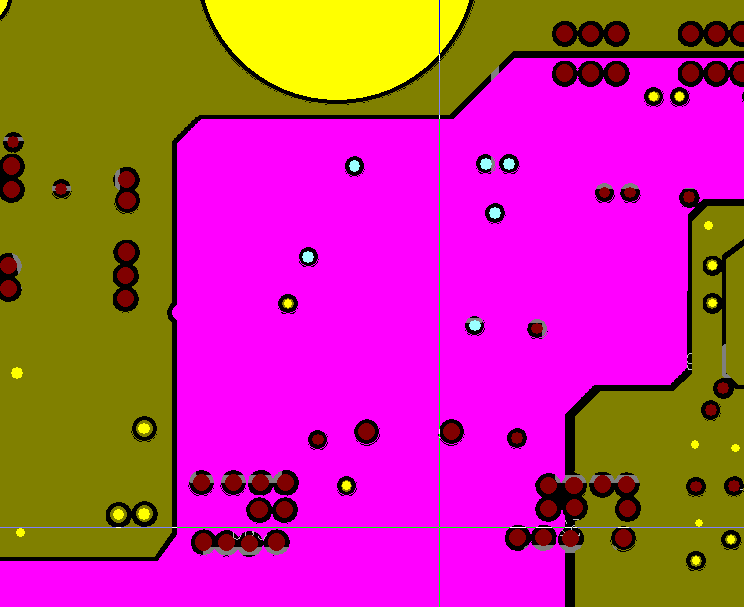
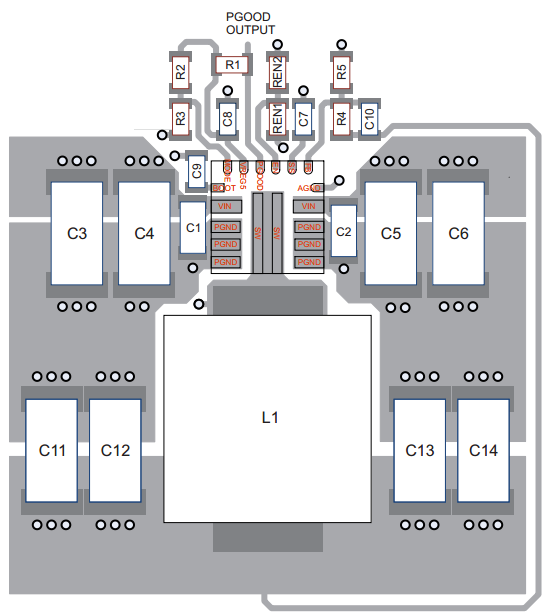
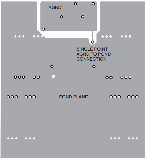
I have questions and concerns using the TPS56C15 on the CPU main board. Looking at the reference design, there are 2 grounds (analog and digital) and combine them at one point. I have it on my CPU board, and with the full system load, the moment we try to change some settings, it resets the board. See below reference.

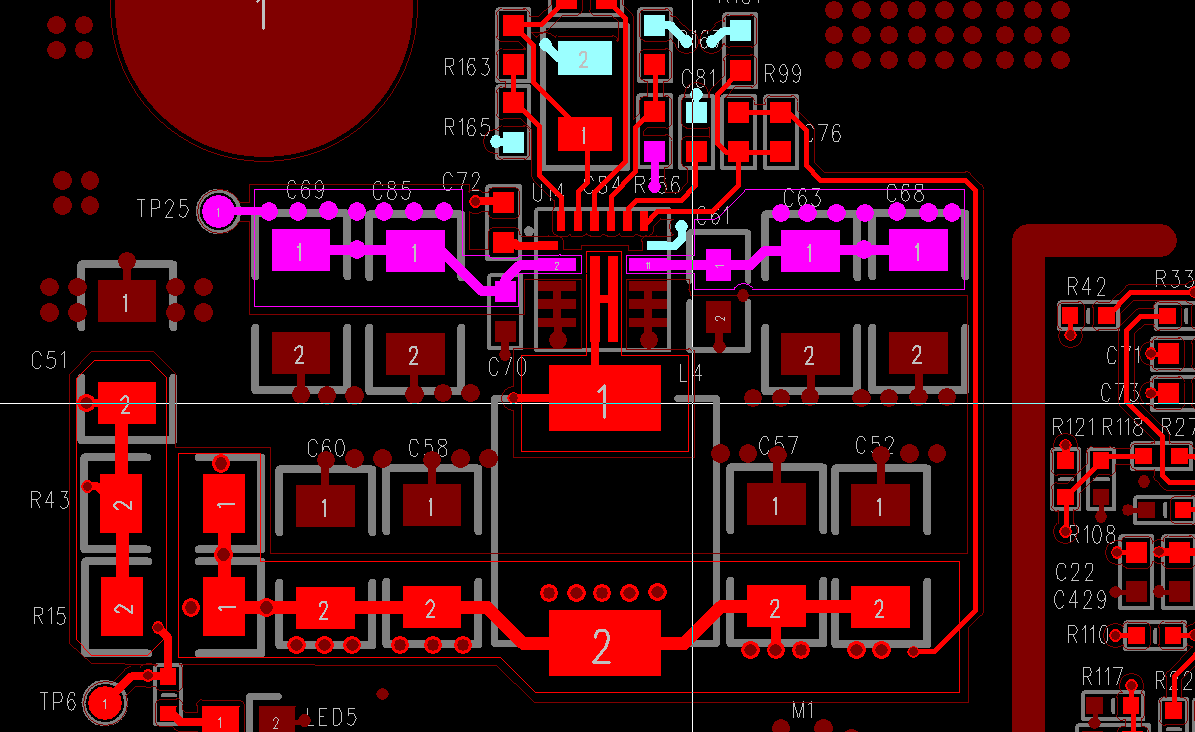
I used marvel supply with no separation of ground, and i never had this issue. See below Marvell, but ignored the 2 grounds, and use it as 1 common ground

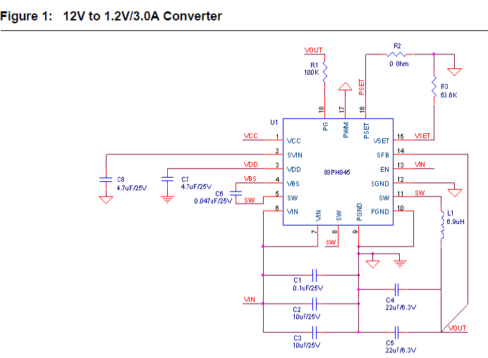
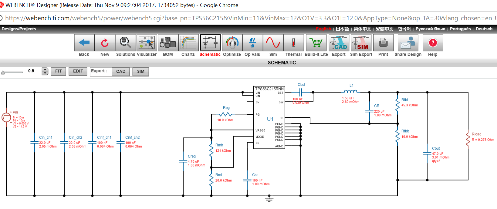
Why are we having this issue if i isolate with 2 grounds,and if i use one common ground, I believe that should able to solve it. From the TI website the workbench showed it as one common ground. see below schematic.

Please help to advise further.

  • Hi,

    2 grounds layout is used on high current applications to improve noise immunity. It's just the same with single ground on schematic level since the 2 grounds are eventually connected through one point. So where you choose as the connection point matters. You can find the recommended layout on the datasheet. If possible, please attach your schematic and layout of TPS56C215 part for us to review.
  • Can you please review this and let me know if i should ignore the two grounds and keep it as one ground? Let me know if this helps, I am wonder whether if i should keep 1 ground or 2?


    See below the schematic


    Top layer


    2nd Ground layer


    Power plane


     Bottom layer (zero ohm resistor you see at the bottom layer to connect analog and digital ground)


  • Hi

    You may not use these vias to connect AGND and PGND, refer to this layout:

    Where are your input capacitors? You cannot use the long path and vis connecting capacitors to VIN and PGND. They should be put on the main current path.

  • Hi Ivan,

    In fact  please see the input capacitors below, input capacitors are very close to the input pins on both sides. I am not using a long path, i am exactly following the layout recommendations.

  • Hi,

    On high current applications, path is nothing but inductors. If the AGND pads is far away from input Cap GND pads which are considered as constant GND, current transient will coupled voltage peaks on AGND and cause errors on IC setup pins. Using one common GND, every AGND pad has a different path to Cap GND, causes the issue worse. So it's better to separate AGND and PGND and your problem will not be solved using single GND.

    Could you please offer the detailed information on your problem? What settings you changed?
  • Hi Iven,

    I can't explain any further, its an error very difficult to visualize and see it. I am changing the design to one common ground and can't wait for TI input. In worst case, I would remove the TI supply and use Marvell like i used before. I don't have time to play with this too much. In the work bench also, they mentioned to have 1 common ground.

    AGND pin is very close to input capacitor, but having a one common ground would have a stable reference for the power i believe. Plus layer 2 is complete GND plane, which would be reference to the AGND pins, so i am not worried for the distance. Let me know your thoughts.
  • Hi,

    Actually the voltages of different point on PGND plane are different when switching due to the impedance and current. If use one common plane, different AGNDs locate on different points of PGND and the AGND references would not guaranteed to be the same. The power current is hard to depict, so I believe using 2 GND planes and finding a single point are safer.

    Since you said the issue resets the board, something unusual should be observed by oscilloscope at the output voltage and switching node when the issue happens. It's difficult to locate the problem without the waveforms.
  • Hi,
    I looked at the scope and nothing unusual happens, it only happens when we connect the 2nd board to the CPU which is our LTE board and LTE is also using another TI supply for 3.8V
  • Hi,

    What is the 2nd board? When it happens, something could be observed at the scope from the power output and switching node.
  • Hi,

    2nd board is the LTE board that we need to connect to our CPU. Keep in mind when i was using Marvell supply this didn't happen. On the scope i couldn't trigger anything to capture, but i would look at it again.
    Can you confirm if I use separate gnds and same ground? Currently, i have changed design to keep it as 1 gnd to make sure the reference point is same.
  • Hi,

    When the issue happens, is output of TPS56C215 full load or other conditions? Is there a load transient? Without waveforms, it's difficult to guarantee which layout can work on your applications.

    Besides, I still have doubts on the connection with AGND and PGND, since the path is long, lies above Vin plane, and Vin noise will have the influence on AGND. You can have the try removing the 0Ohm res and connect AGND and PGND with a very short wire just on the first layer. The wire should be kept away from switching node.