This thread has been locked.

If you have a related question, please click the "Ask a related question" button in the top right corner. The newly created question will be automatically linked to this question.

LM3150: Vout and Ripple too high, increasing with Vin

Part Number: LM3150
Other Parts Discussed in Thread: ALLIGATOR

Hello all,

I'm currently struggling getting the LM3150 running. Three voltages are planned: Vout 3.3V, 5V and 12V, Iout: 6A. Vin 12-24V (Vin > 15V when Vout = 12V). The schematic is based on Webench, with minor deviations (3.3V version shown here):

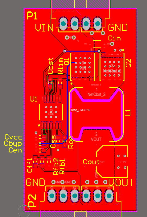
(GND polygon on bottom layer hidden. Pink shape under inductor is a keepout area on the top layer)

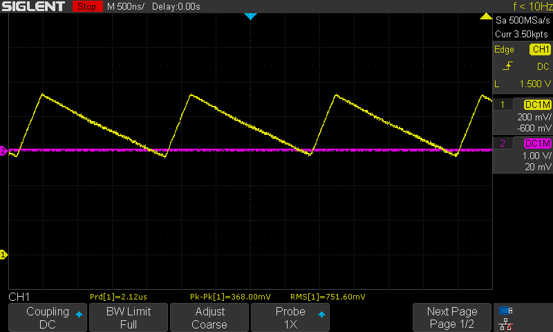
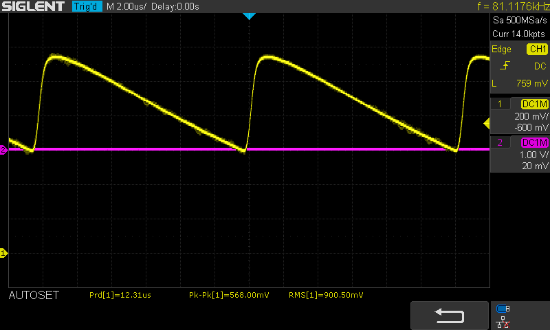
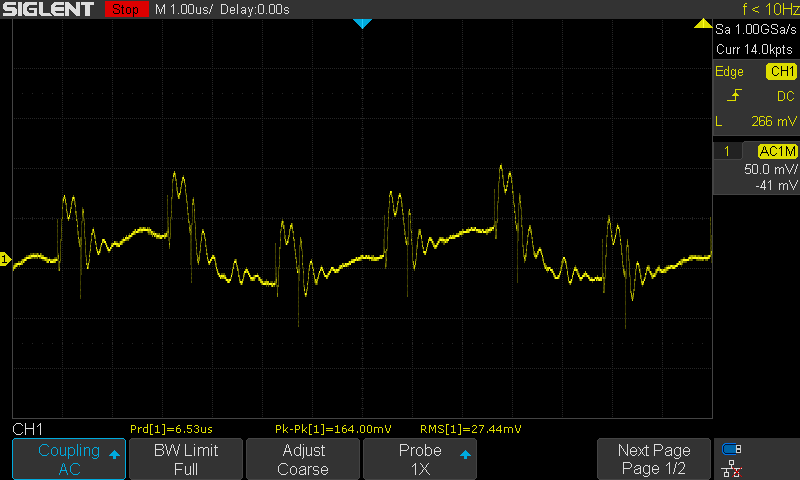
Under test, both the output voltage and the output voltage ripple increase steadily with input voltage. When supplied with 24V those values become way to high, for example up to 4.1V RMS and nearly 400mV peak-to-peak in case of the 3.3V regulator.

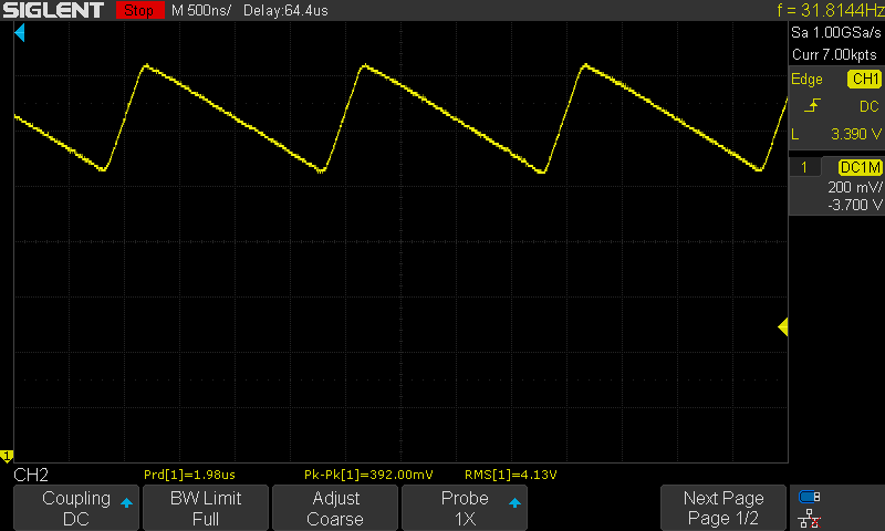
(Note Ron increased from 75k to 100k on this test, which didn't exactly help)

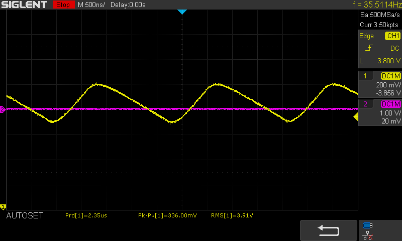
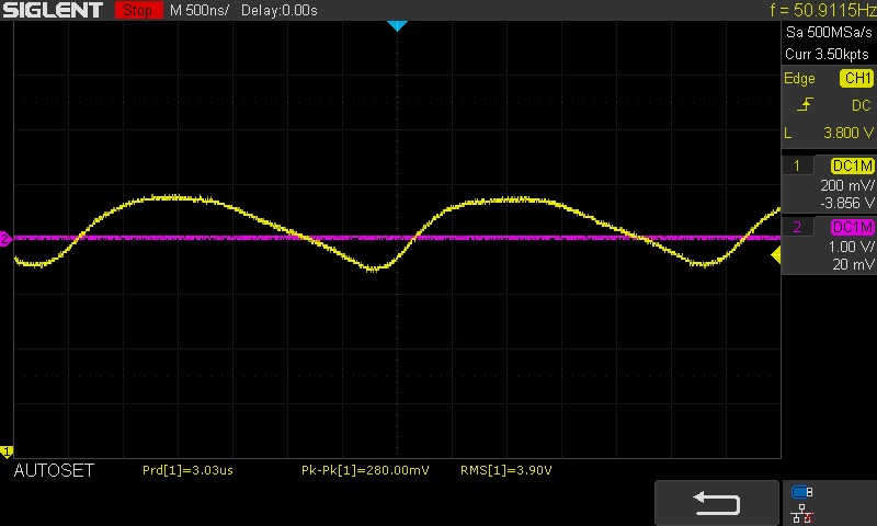
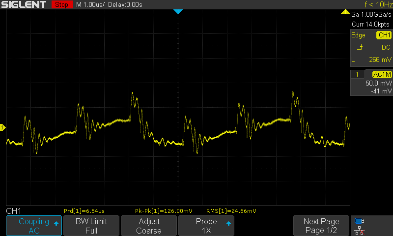
Increasing the inductance to 10uH and removing Cff (560pF appears high, compared to the example from the datasheet) reduces the symptoms somewhat. Adding load (2Ohm wire wound resistor) didn't change things much.

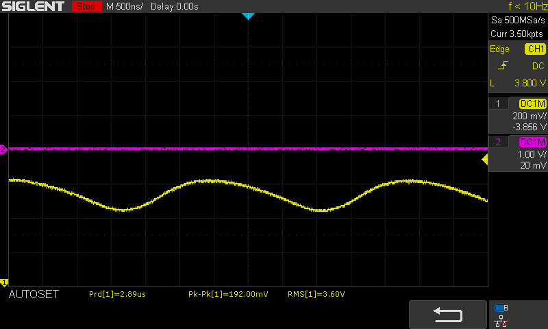
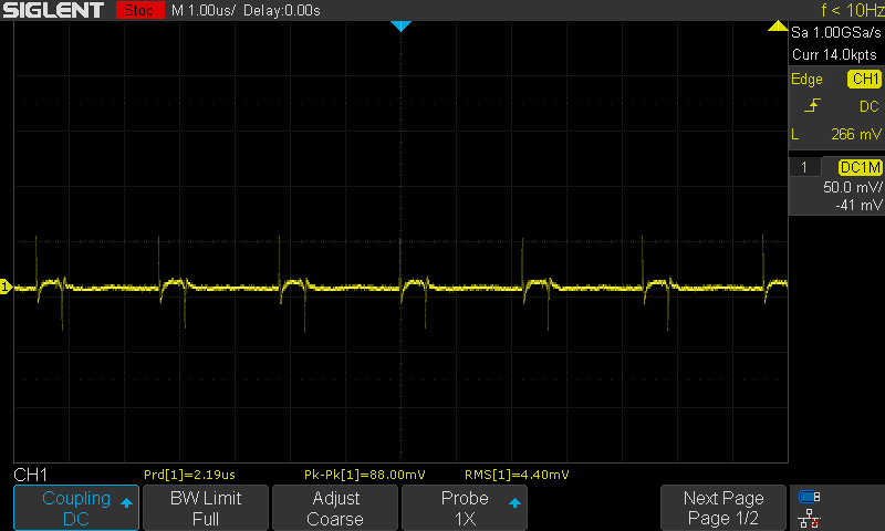
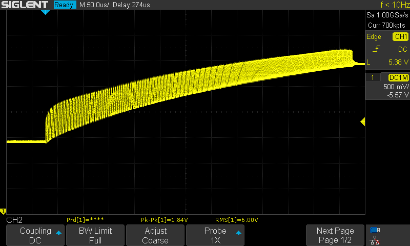
Another particular issue is the 5V regulator. It appears to be running in a discontinuous mode with short periods of switching ending in a too high output voltage followed by a decay to the nominal value over about 1 second. The other regulators don't exhibit this behavior.

As of now, I'm out of ideas what to try next, so any help is appreciated!

Best Regards

Reinhard

  • Hello Reinhard,

    I have forwarded you post to the responsible person covering this device. They will respond shortly.

    Thanks for your patience.

    David.
  • Hi,

    are there any news? Sorry for being impatient, but the buck converters are the final roadblocks before we can proceed with the project.

    Thanks!

    Reinhard

  • Reinhard,

    Sorry for the delay.

    1. First let's try probing the FB pin. This way we can see what the IC is getting.

    2. I also recommend adding a low-value HF ceramic cap on the output. 1uF should be good.

    3. You can also try connecting FB to VOUT at the + terminal of the bulk cap. This can be done on the bottom layer of the layout, or for testing now, cut the trace and fly a wire to that terminal.

    4. Cut the SGND copper at the pin so the SGNDs only connect to the DAP under the IC and nowhere else. Noise might be coupling in through those SGNDs.

    I'll keep thinking on this. Get back to me and we'll continue the debug.

    -Sam
  • Thanks a lot for your response!

    1) This is how the FB pin looks (Vin24V, Vout 3.3V). The ripple amplitude is similar to Vout.

    2) 1uF on Vout makes the ripple even a bit worse.

    Vfb

    Vout

    Going further and adding a ceramic 10uF capacitor will reduce ripple and voltage error a bit.

    Vout

    and Vfb

    3) Connecting Cout directly to FB, therefore setting Vout to 0.6V (please correct me if I misunderstood your intentions here)

    4) Cutting the GND plane just outside of pin 5 and 9 (SGND) had no noticeable effect, but it is kinda hard to see if I cut it completely.

    On a side note, after making these tests I connected it in again and the magic smoke left the LM3150, which is now visually damaged next to pins 2 and 3. This LM3150 previously became too warm when operated at Vin=24V, so it might have been already damaged by all the tests. I need to build up some new test boards.

    So far, I don't see a solution in sight. Maybe adding a big (>=100uF) ceramic capacitor to the output is a useful workaround, but I don't feel this addresses the core issue on my design.

    Reinhard

  • Reinhard,

    I agree, we need to get to the root cause of this issue.

    I'm wondering about the layout with regard to grounding. Can you take scope shots of:

    • VCC pin of ICwith respect to GND on P1 and P2
    • VIN pin of IC with respect to GND on P1 and P2
    • SGND1 pin of IC with respect to GND on P1
    • SGND2 pin of IC with respect to GND on P1

    Thanks,

    -Sam

  • Sam,

    After the last board died, I built up a new one. It doesn't contain any of the above mentioned test modifications (e.g. cutting the GND polygon outside SGND or the ceramic capacitor on Vout).

    The first screenshot is always with respect to P1. Due to the bigger distances, these measurements were all made with a ground lead on the probe (alligator clip), compared to the previous with a ground spring, so they might contain more noise.

    VCC pin of IC with respect to GND on P1 and P2

    VIN pin of IC with respect to GND on P1 and P2 (DC coupling, not much to see here)

    VIN pin of IC with respect to GND on P1 and P2 (AC coupling, not much to see here)

    SGND1 (pin 5) pin of IC with respect to GND on P1 an P2

    SGND2 (pin 9) pin of IC with respect to GND on P1 and P2

    Thanks again!

    Reinhard

  • Reinhard,

    Yes, this is looks to be caused by the layout. Here are my thoughts:

    • Move CVCC up and to the left a bit to fit VCIN very close to the pin.
    • Place FB resistor very close to the pin
    • Use a thicker trace to VIN. If voltage on that trace has large enough ripple, use separate trace for Ron.

    In general

    • Reduce loop area on high di/dt traces
    • Reduce trace area and proximity to other sensitive traces on high dv/dt traces

    And you can see the layout guidelines for general rules and recommendations.

    -Sam

  • Thanks a lot, Sam!

    I've adjusted my layout as suggested by you and will see how the next revision works out.

    Reinhard