This thread has been locked.

If you have a related question, please click the "Ask a related question" button in the top right corner. The newly created question will be automatically linked to this question.

TPS65218: TPS65218 INT_LDO

Part Number: TPS65218

Hello all,

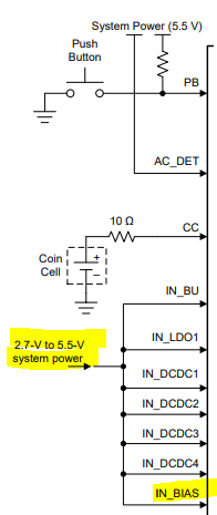
Our customer measured TPS65218 by using theirs EVM. When VIN is forced, DCDC3 is 0v to 0.7V, 0.7V to 0v and DCDC3 is ramped.

It's strange behavior. TPS65218 goes to ACTIVE mode with no issue. When INT_LDO is remained above 0.6V, strange behavior is occurd. When INT_LDO below 0.6V, strange behavior isn't occurd.

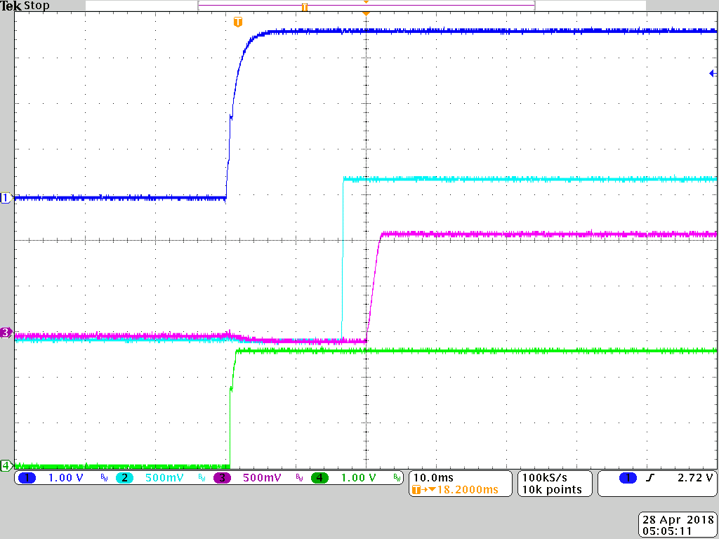
Is strange behavior OK? Or Do you have any solution? I attachied strange behavior  
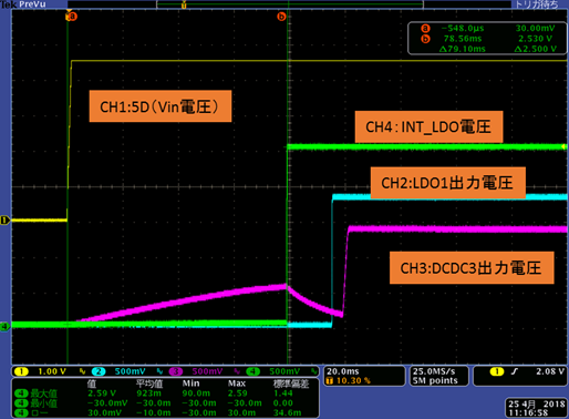
wave.  CH1: VIN CH2: LDO1 CH3:DCDC3 CH4:INT_LDO

Best Rgards.,

M.Iwasaki   

  • Hi,

    This thread has been assigned to an application engineer who will get back to you shortly.

    Thanks,
    Nastasha
  • Iwasaki-san,

    Please tell me if customer using TPS65218 (ending in -B1 or -B101) or if they are using TPS65218D0.

    The -D0 version is the final version of silicon and is recommended for use in all new designs. Many issues identified in -B1/-B101 version of silicon were resolved in -D0.

    The issue you have identified could be related to an application problem, but it will be helpful to identify the full Part # used by your customer before we begin to debug.
  • I have attempted to re-create your issue on a TPS65218EVM-100 board and it appears that the reason for your issue is because IN_BIAS is not connected directly to VSYS. There is a delay between VSYS and INT_LDO on your scope shot, and INT_LDO is generated from IN_BIAS.

    When I tested, I captured my signals on the same channels as in your testing, but the scope converts channel 1 from Yellow to Dark Blue.

    You can see that Channel 4 (INT_LDO) in my scope shot rises at the same time as VSYS (Ch. 1):

  • I am using TPS65218. You means that TPS65218 is occured unstable DCDC1-3? TPS65218D isn't occured?
    If correct, Why is there TPS65218 on TI WEB site?

    Best Regards.,
  • Hello Brian,

    I understood it. Should I connect IN_BIAS to VSYS directly?

    Best Regards.,
    M.Iwasaki
  • Yes, IN_BIAS should be connected directly to the main "System Power" supply, which you labeled VIN on your scope shot.

    IN_BIAS is a sense pin for UVLO in addition to being the supply for INT_LDO and the bias voltage for all DC-DC converters. The PMIC does not expect the IN_DCDCx, IN_BU, or AC_DET signals to ramp before IN_BIAS.

    The Typical Application Schematic (Figure 6-3 on page 93 of datasheet) shows all the inputs that should be connected directly to the "2.7-V to 5.5-V system power" supply:

  • The TPS65218 -B1 and -B101 silicon versions are in the process of being set as NRND and the TPS65218D0 will be the only ACTIVE device moving forward. The -D0 version just released in Nov 2017 and the NRND process can take time to complete.

    I cannot say if TPS65218 -B1 and -B101 silicon is the root cause of this issue because I did not test the case where IN_BIAS ramps after the main system power supply (VIN or VSYS). This use case is not allowed by the datasheet and is outside of the specifications of the device.

    I am simply saying TPS65218D0 device should be used for new designs because it is newest silicon version.
  • Hello brian,

    We will recommend TPS65218DO to our customer. When they use TPS65218DO from TPS65218, Can they use the same schematic?

    Best Regards.,
    M.Iwasaki
  • Iwasaki-san,
    Yes, the TPS65218D0 is pin-2-pin and functionally equivalent to the original TPS65218 (-B1 silicon).
    -D0 silicon is simply a new and improved version of the same device.