This thread has been locked.

If you have a related question, please click the "Ask a related question" button in the top right corner. The newly created question will be automatically linked to this question.

UCC27714: UVLO fault, how can I open the HO gate to HS source? Please help me

Part Number: UCC27714
Other Parts Discussed in Thread: UCC2895

I bought some UCC27714 half-bridge driver to make a piezo high voltage driver few weeks ago.In my testing period, I encountered some problems. One is that the HO output is abnormal.

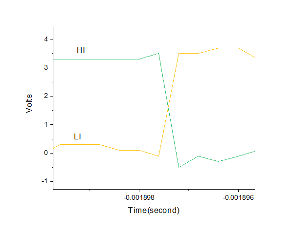
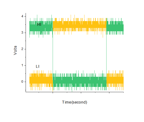
If I give a period rectangular wave that is HI and LI change from 0 to 1 periodicly. I find that the LO response is right. But the HO response is always the Vgate(Voltage on the FET’s gate pin) is equal to Vsource(voltage on source pin).My diagram is like this:

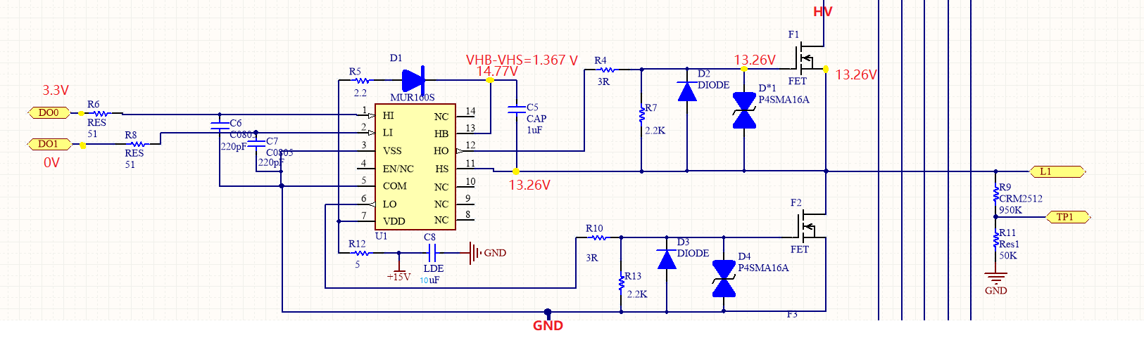
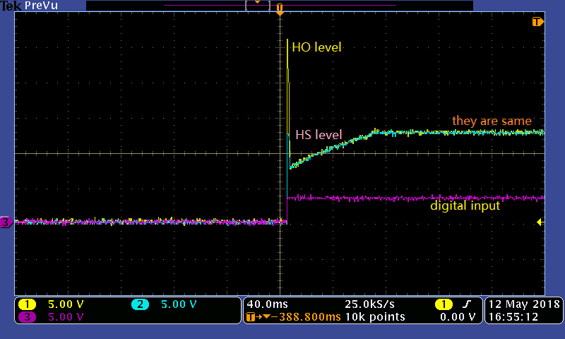
The yellow points represents test points. The red values are the tested values. I think this is UVLO fault. But I don’t know how to solve it.

Please give some tips. Thank you very much!

  • Hello User5329003,

    Notice HS make HO output very high during Cboot charge. It would seem HS is not being pulled to ground in start of bootstrap cycle?

    We posted similar captures this forum last few weeks, HS jumps to HO etc... The HO/LO (GTRon = 3R) may be a bit low value even @IGPK+/- 4 amp <10us pulse short to ground. This seems to stress HS during Cboot charge cycle. Cboot then remains mostly as floating voltage on HS -- after seems to leak output current onto Cboot forevermore.

    Advise to replace UCC27714 with new gate driver and factor 6-8x total NFET QG for GTRon value (18R-24R) adding some safety margin. Perhaps reduce/increase GTRon as your PWM frequency design allows without destruction occurring to UCC. Always good to see circuit work for awhile and watch it crash then have a silent theft nobody to witness the crime.
  • user5329003 said:
    If I give a period rectangular wave that is HI and LI change from 0 to 1 periodicly

    You mean to say the HI/LI are complementary PWM signals?

    BTW: Might R7-13 2R2k produce some undesired roll off rising edge of high frequency gate drive? Typical value 10K/20K, considered safety GTRoff, shut down NFET if HO/LO is lost from open R or open copper trace.

  • Hi,

    It looks like your bootstrap cap, C5 isn’t getting charged. You need to drive HI and LO with a constant PWM signal, otherwise the bootstrap cap will get discharged due to the gate leakage of your mosfets. If you run it at 10-20 kHz, do you see this same issue?
  • I want to increase my input frequency but my device's bandwidth can't reach that range. I used a 300Hz PWM signal to try its performance and it failed again. Because the dropping time scale is shorter than 2ms. Could you give other scheme? Thanks!

  • Yes, when HI is high,and LI will be low.
    I will try your advice. Thanks !
  • By the way, could you tell me how to check my driver ( it is good or broken)?
  • Hi,

    I'm of the belief Cboot is properly charged by LO during 1/2 bridge dead time periods in HI/LI PWM signal. Not all simple schemas can do that without complex handling of HI/LI drives.

    As Don injected it must be insured LI toggles (high) produce Cboot charge time prior to toggling HI (high) or no output power will result from HO driven NFET. Hard to imagine if LI was not toggled prior to HI how that might lead to HS being stressed.

    If you are using a function generator can it insert dead time periods between the HI/LI drive input times? If not the UCC2895 can generate signals you need, check the frequency range it allows.
  • Hi,

    What does your waveform look like at 300 Hz?

    I think maybe R7 is too big. Can you remove it and see if it works correctly?
  • Thank you for your tips! I will keep in mind. You are cool! Your tip that replace 2.2k resistor with 20k worked but new problems occurs. Anyway, thanks a lot. I will update the new test results.
  • Thanks, I will update the waveform and try your solution.

    Bests
  • BTW:
    After R7-R13 change 20k or remove per DON's suggestion when LO turns on HS pin should go to ground on scope capture. If HS only moves slightly down or half way from 13.6v when LO is above NFET gate threshold, the UCC is likely damaged. LO should pull HS or Cboot all the way or very close to ground prior to asserting the first HI drive pulse/s.

    We allow milliseconds of LO side PWM pulses 1% duty cycle to charge Cboot then commutate HI/Li sides powering the inductor. Typically good efficiency results from 2 UCC working together in zero voltage switching schema.
  • Hi,

    The waveform is like this


    I have tried to remove the 2.2K resisitor and it works normally and the HO can maintian high within 60ms. 

    Due to I never used half-bridge driver, could you please tell me when the HO is higher than HS, and FET1 opens, FET2 shut down, HS becomes a very high state(HV). Now, how the HB pumps up to higher than HS and then HO will become same to HB. Thus, the FET1 can maintian the on-state.

    Does it only through the boot capacitor or the internal circuit?

    Really appreciate you!

  • Hello user5329003,

    The HB-HS voltage is maintained only by the bootstrap capacitor. There is no internal circuit to charge the bootstrap capacitor, so periodically HS must be brought to GND to refresh the charge on the bootstrap capacitor through the external diode connection.

    When HS goes to HV, there will be three elements that decrease bootstrap capacitor voltage:

    1. Gate charge of the high-side MOSFET. Cboot voltage will decrease once per cycle, during turn-on of HO. Since C = Q/V, Vdrop = Qg/Cboot.
    2. Clamp resistor R7 current. Voltage decrease will follow R-C exponential behavior, with time constant of R7 * Cboot.
    3. Quiescent current of the IC. Treat as a current source using datasheet values, and since I = dQ/dt, Q = I * t and Vdrop = (I * t)/Cboot.

    If the sum of these losses causes the HB-HS voltage to drop below UVLO threshold, then Cboot or R7 could be increased as potential solutions.

    Regards,

  • Awesome! I need this detail explanation! You’ve been so helpful.

  • Hi Derek,

    Derek Payne said:
    Clamp resistor R7 current. Voltage decrease will follow R-C exponential behavior, with time constant of R7 * Cboot

    Where did you derive such information as no other vendor suggests the protection resistor (R7 in this case) has any influence on Cboot RC time constant?

    It would seem the discharge current path of Cboot RC time constant is what you are referring to, so R7 only has partial influence but only during discharge?

  • Hi BP101,

    In case it was unclear, the current through the protection resistor is only present when the output is high.

    At higher frequencies (>20kHz), the R-C time constant from the protection resistor is usually much larger than the switching period. For example, a 2.2kΩ resistor paired with a 1µF bootstrap capacitor would have a time constant of 2.2ms, compared to a period of 50µs; this represents a change of e^(-t/RC) = less than 1% of the bootstrap capacitor voltage, even at 99% duty cycle. But at lower switching frequencies (such as 300Hz in this application), 50% duty cycle would cause about 28% drop in the bootstrap capacitor voltage, and 99% duty cycle would be about 55% drop in bootstrap capacitor voltage, with the same bootstrap capacitor and protection resistor values. This is probably why other vendors have not suggested any meaningful influence: motor drive, power supply, and inverter applications all switch at frequencies where the protection resistor doesn't have much influence on the bootstrap capacitor selection.

    Regards,