Because of the Thanksgiving holiday in the U.S., TI E2E™ design support forum responses may be delayed from November 25 through December 2. Thank you for your patience.

This thread has been locked.

If you have a related question, please click the "Ask a related question" button in the top right corner. The newly created question will be automatically linked to this question.

TPS28225: Charged Depleted during 300kHz PWM at 50% Duty Cycle?

Part Number: TPS28225

Hello,

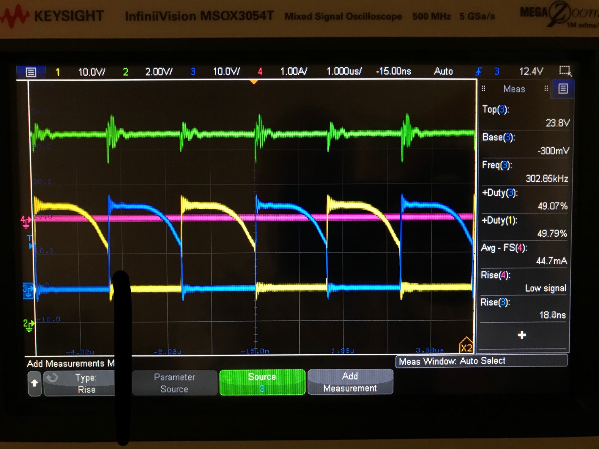
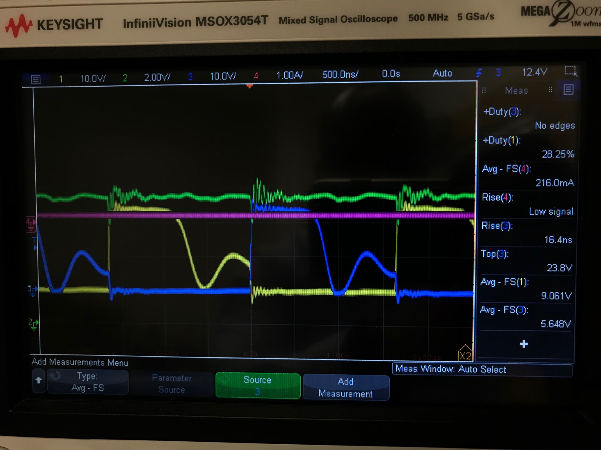
I have a TPS28225D on a board in a full bridge application. I am driving Qty:4 IRFR7446TRPBF MOSFET with a 5%-95% 300kHz PWM into a 0.25-2ohm load. I am currently have a problem that seems as though the gate driver is depleting its charge and dropping off after 1us at 24V. The feedback buck resistor and capacitor were initially 2ohm and 0.1uF. I then changed the the feedback loop to 0ohm and 0.22uF hoping it would add additional charge to sufficiently drive the gate. This was not the case. What might I be over looking to make sure my gate is fully driven for the full PWM cycle?

Image 1 (300Khz - 50% Duty Cycle, IRFR7446TRPBF (CASE1 - Simple Droop))

Image 2 (300Khz - 50% Duty Cycle, STD25N10F7 (CASE2 - Droop with recovery)

Image 3 (A Side Driver Schematic)

BLUE - High Side A @ T56 (Phase A)

YELLOW - High Side B @ T73  (Phase B)

PINK - Current into 2ohm

Thanks,

Darnell

  • Hi Darnell,

    Welcome to e2e and thanks for your question. Sorry to hear about the issues your having with TPS28225, I am an apps engineer with this device and hope to help out.

    I have a few clarity questions first:
    what is the green waveform? it appears noisy.
    what nodes are the four waveforms of exactly? what is highside A/B? is highside A = UGATE and highside B = LGATE?
    what is the 2ohm pink current waveform? is this the bootstrap resistor current?

    if BOOT voltage is drooping - it looks like Cboot (0.1uF) is discharging at a rate of about 10V/500ns this equates to a 2A peak discharge current which is too high to be leakage. What we need to see what the voltage on BOOT is when the highside turns on, it would help to see what PHASE and HI voltage is during this test. If the BOOT voltage is getting depleted halfway through the 4us period with a discharge current of 2A it could mean that the device is may be sinking unwanted current from excessive negative or positive transients on PHASE node that may affect the BOOT voltage rating.

    Thanks,
  • Green is voltage at T57 with no ground reference (hence noise). Pink is current at T57. Blue and Yellow are voltage at T56 (A Side)  and corresponding node on B side of the full bridge.

  • Hi Darnell,

    Thanks for the reply.

    I see, Id like to see a scopeshot of UGATE, BOOT, PHASE and P24V on the same plot showing a few cycles of the issue. We will determine if the waveforms meet ds ratings.

    Did this issue pop up or has it been always like this?

    Do you the identical setup driving side B?

    What fets are you using?

    What is you end equipment or application? How is the issue affecting your system?

    Is price the reason for choosing tps28225 for your application?

    Thanks

    Jeff

  • Please see the details and images in the original post. I think these answer most of your questions. The scope plots are from two different boards. FET details are included. What’s the reason for not choosing the TPS28225?
  • Hello Darnell,

    I am an applications engineer who works with Jeff, who you have had previous communication.

    The scope captures you indicated are Blue Switch Node A (or Phase A), Yellow Switch Node B (or Phase B), Pink current into 2 Ohm (we assume R29), and green Vout T57.

    To determine why the half bridge switch node is showing the voltage droop, can you provide some additional waveforms?

    If the A and B behavior is the same, you can concentrate on one phase. Please show the following waveforms, with scope probes referenced to ground. T53 (UGATE), T56 (PHASE), T63 (LGATE) and BOOT. The same time scale and conditions as your original plots should be OK.

    We also need to see if the current in L3 is continuous or DCM which will affect the waveform on T56. Can you also get scope plots of  T53 (UGATE), T56 (PHASE), T63 (LGATE), and L3 current with the same scale and conditions as above.

    We need to see the relationship of the bootstrap bias (BOOT), and high side drive (UGATE) relative to PHASE since those voltage are referenced to PHASE. We want to determine if the high side drive bias and output are drooping, relative to PHASE, to determine if the high side FET has adequate drive voltage.

    Can you tell us the values of R28/C82 and R35/C86 snubbers? With some more information, we can help explain the cause of the waveforms in your application.

    Regards,

    Richard Herring

  • Answers below. Thanks.

    R28/C82 and R35/C86 are spare, unstuffed, NOPOP.

    Blue and Yellow of original plots are A and B phase of the two different boards described in the original post.

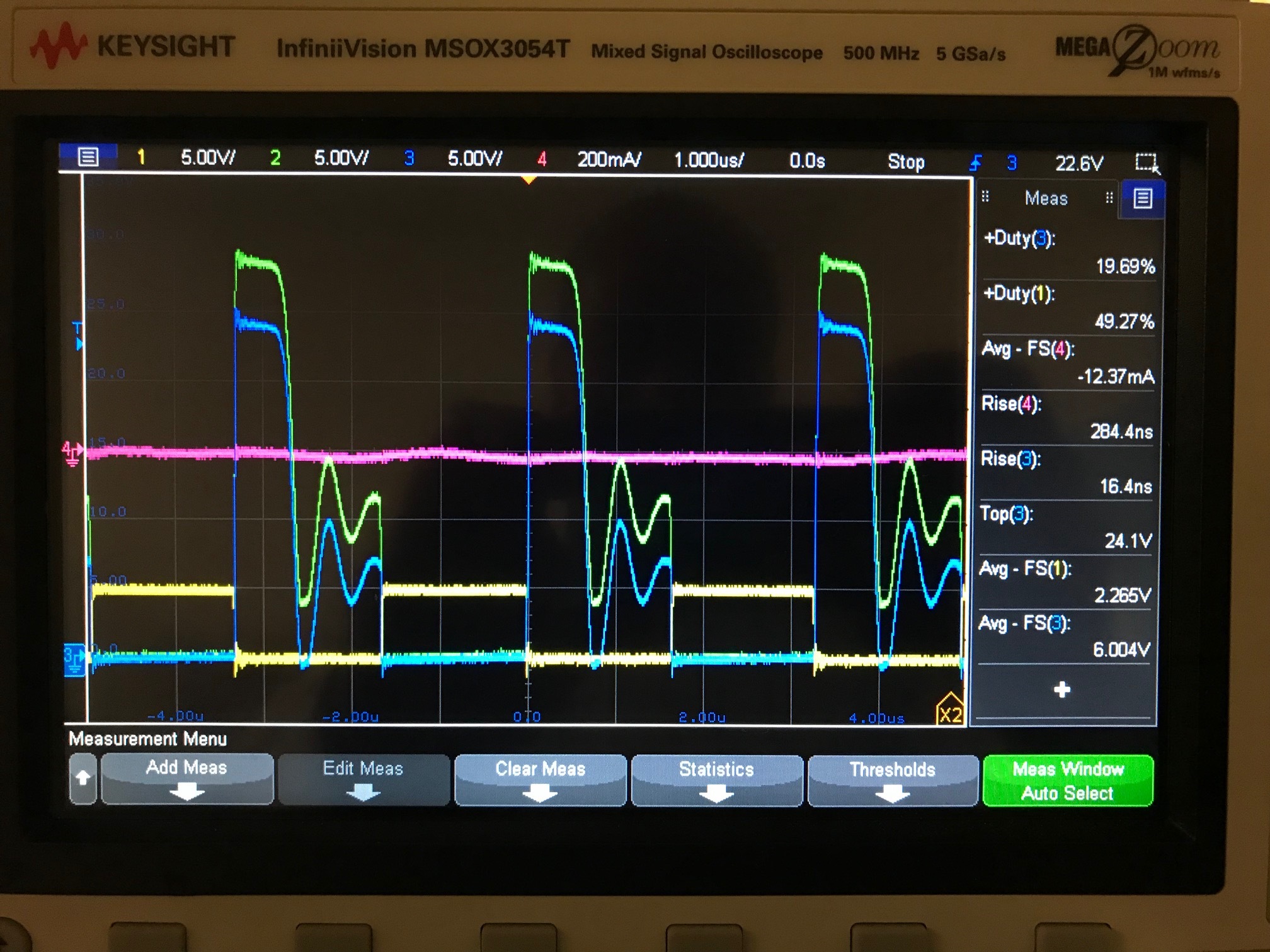
    New Capture as requested: GRN T53 (UGATE), BLUE 56 (PHASE), YEL T63 (LGATE), PINK I_T57 (L3 current)

  • Hello Darnell,
    I should have mentioned to make the scope plots more clear, to have UGATE and PHASE on the same voltage scale and ground reference. What you will see will be UGATE higher than PHASE during on period and on top of PHASE during off period.
    One thing I see which makes me curious to see the overlap plot, is that when PHASE rings to ground, UGATE is ~5V above ground, which indicates UGATE is high relative to PHASE.
    Since the TPS28225 has a tri state feature, I am curious what the PWM input signal is doing.
    Can you provide a plot of UGATE and PHASE same scale, same ground reference, PWM input, and L3 current.
    Second plot same conditions with UGATE and PHASE same scale & ground ref, PWM input and LGATE output.
    The ringing on PHASE does not look as expected when the L3 current is always >0.

    Regards,
    Richard Herring
  • See updated image above. PHASE follows UGATE as expected. Thanks.

  • Hi Darnell,

    Thanks for your update, it looks like the highside and lowside FET are getting the proper drive through out the switching cycle.

    the inductor ripple current however is not lining up. Is there supposed to be load current through the inductor?

    Can we see if the input are OK? Can you do a similar scopeshot of PWM, EN/PG with PHASE and UGATE?

    Thanks,

  • Hi Darnell,

    any update with this issue?
    If not I will assume its resolved, feel free to repost to repoen the thread.

    thanks,