This thread has been locked.

If you have a related question, please click the "Ask a related question" button in the top right corner. The newly created question will be automatically linked to this question.

LM5122: Forced-bypass operation

Part Number: LM5122

Hi all,

I need to design a DCDC converter with the following specs:

-Vin=6 to 12V nominal (to withstand automotive cold crank)

-Iout = 10A

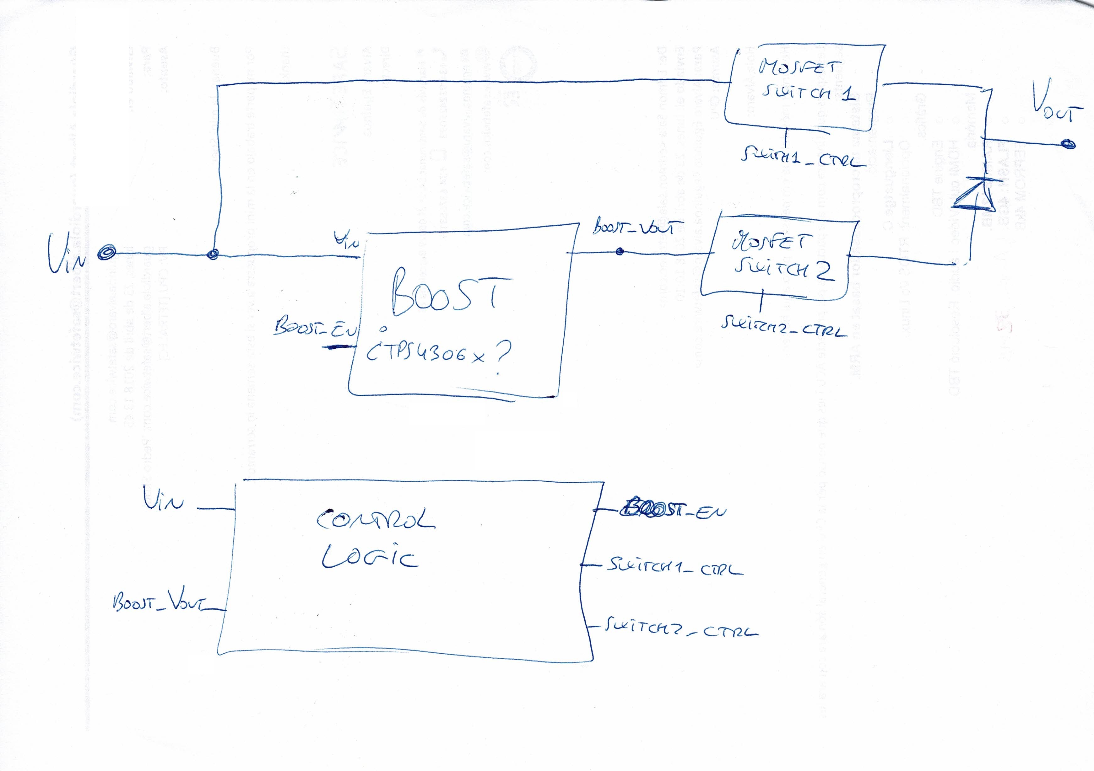
-Here's the tricky part: If Vin<11.7V then FAN48623 Vout=13.2V; if Vin>11.7V then Vout=Vin). 

So I cannot use straightforward the bypass function included in LM5122, since my Vin threshold to enter bypass is not the same as the Vout target value. Therefore, I would need a controller that includes a "forced-bypasss mode" (let's say, with a dedictaed pin, such as Fairchild's FAN48623). Could you recommend some Texas controller that would match these specifications? If not, any app note that comments on this peculiar scenario would also help.

Best regards, thanks indeed

  • <Errata edited>

    Hi all,

    I need to design a DCDC converter with the following specs:

    -Vin=6 to 12V nominal (to withstand automotive cold crank)

    -Iout = 10A

    -Here's the tricky part: If Vin<11.7V then Vout=13.2V; if Vin>11.7V then Vout=Vin).

    So I cannot use straightforward the bypass function included in LM5122, since my Vin threshold to enter bypass is not the same as the Vout target value. Therefore, I would need a controller that includes a "forced-bypasss mode" (let's say, with a dedicated pin, such as Fairchild's FAN48623). Could you recommend some Texas controller that would match these specifications? If not, any app note that comments on this peculiar scenario would also help.

    Best regards, thanks indeed
  • Hi Albert,

    There is not a device that has the functionality that you need with respect to that application parameters. One solution would be to shift the target output voltage when needed to pull the device into bypass mode. This could be done by using a few MOSFETs and extra resistors in the resistor feedback divider. for this application is there signal that tell the device to go into by-pass mode? Or does it need to trigger independently?

    -Garrett
  • Hi Garrett,

    Thanks for your comment.

    The device shall go into bypass-mode when the input voltage is above 11.7 V. That's the "signal" we can use to shift the operation mode of our device.

    Considering your proposal (shifting target Vout): I'm concerned about the commutation between bypass-operation and non-bypass operation. It shall be no slower than 10 us, with only a 3% Vout voltage regulation... at 10 Amps.

    Regards
  • Hi Albert,

    I would be worried about meeting the 10 us slew rate. I don't think that would be possible with my suggestion. Let me think there is another way to enter bypass mode. I will get an answer back to you shortly.

    -Garrett
  • Hi Garrett,

    Thanks for your help, I will be looking forward to your answer.

    Here i have come up with an "external bypass" arrangement, please let me know your view:

    -I am considering a controller such as TPS4306x that come swith an ENABLE pin (datasheet: tEN :EN to start switching time) 125 uF). Let's keep this in mind. This is the considered architecture:

    -Vin range goes from 6V to 12V, nominal is 12V, that is above 11.7V, which is the lower threshold to enable bypassing. So nominally, the device is in bypass mode.

    -A transient occurs (automotive motor crank) and Vin goes down from 12V to 6V in 6 ms and stays there for about 1 s.

    -Below Vin=11.7V, the device must shift to boost mode, and Vout target must be set to 13.2 as specified (see my first post).

    -A simple control logic would be enough to turn SWITCH1 off and SWITCH2 on properly so Vout is hold. The problem is commutation time.

    -So here's the proposed control for a two-step shift to boost mode.

    1.When Vin drops below the Vin threshold, BOOST circuitry is enabled (BOOST_EN=1) but SWITCH1_CTRL remains on and SWITCH2_CTROL remains off.

    2.When Vout reached target BOOST_VOUT, Vout is switched to BOOST: SWITCH1_CTRL goes oof and SWITCH2_CTRL goes on.

    What am I concerned about? That the two-step shift to BOOST mode implies that

    1.First, the BOOST starts switching with no load.

    2.Then, when target BOOST_VOUT is reached, a 10A load is connected to the BOOST. How will the regulation work?


    Please make your comments. And let's hope you come up with a more built-insolution (perhaps using LM5122 as initially considered).

    Regards

  • Hi Garrett,

    Any updates on this?

    Thanks, best regards.

  • Hi Albert,

    I still have not come up with a good way to meet the 10us response requirement. The approach described using the switches might have a hard time meeting this requirement as well.

    Can you explain why you need to higher voltage requirement during cold crank. Typically in this application the boost converter is just there to keep the voltage above something like 10V.

    -Garrett
  • Hi Garrett,

    The 13.2V target for output voltage is an specification coming from the client. They need to keep some radio unit running.

    "The approach described using the switches might have a hard time meeting this requirement as well." Why would it be?

    Best regards
  • Albert,

    The concern is how fast the from sensing the input voltage changed to turning on the switch to power from the boost converter. It depends on how the voltage levels are being sense. If a micro-controller is being used it might be hard to meet the requirement.

    There will probably be a dip on the output voltage (13.2) when the switch is turned on for two reasons. The response of the TPS40360 since it operates in DCM at no load. The other being the load is 10A. Adding extra output capacitance will help to reduce this dip.

    Thanks,

    Garrett
  • Hi Garrett,

    Thanks for your comments, I will keep them in mind.

    We have decided to start designing with LM5122 (since we have used it earlier), and prepare different control strategies so we can test them on prototypes. But Webench tool can't calculate a design for our inputs (can't find proper FETs). We are setting Vin=6 to 12V, Vout=13.2V and I=10A as inputs. 

    Is there any workaround to help us with the calculations?

    Regards

  • Hi Albert,

    One trick to to lower the temperature. Sometimes this will help WEBENCH find a FET that is in the library. At ~130W the design might require two FETs which WEBENCH does not support at this time. If you have any more questions please let me know.

    -Garrett
  • Hi Garrett,

    Any comments on Webench limitation for our specs? Any workaround / spreadsheet tool?

    Best regards

  • Hi Garrett,

    Regarding the LM5122's automatic switch to and from bypass mode, when Vin=Vout_target): are there any estimates for switching times?

    Regards
  • Hi Albert,

    There is not a spreadsheet tool for the LM5122. As I mentioned WEBENCH might not be able to find a MOSFET in the library that will work. That does not mean that there is not one that will fit the application. Did you try lowering the temperature as I mentioned?

    Normally the transition time between switching and bypass mode is about 1 switching cycle. This is due to how the bypass mode is implemented internally.

    -Garrett
  • Hi Garrett,

    I'm sorry: totally missed your post on May 30, 2018 1:33 AM.

    Taking your advice: Webench has managed to build a design with Vin=5 to 12V at 0 degrees. I'm assuming that I can used it for our design, but surely i will have to oversize FEts. i have calcultaed power dissipations of 2W for each of them. We are using TO220-like FETs with the body attached to an aluminium body for dissipation.

    Regarding the alternative of using the two-FETs startegy: could you refer us to an app note that illustrates the idea? It'd be much appreciated.

    Thanks, best regards

  • Hi Albert,

    There is not a dedicated application note for on this topic. What I am proposing is just adding a resistor in parallel to the bottom feedback resistor that can be toggled on and off with a switch. This is just a simple way of implementing a variable output voltage design.

    Thanks,

    Garrett