This thread has been locked.

If you have a related question, please click the "Ask a related question" button in the top right corner. The newly created question will be automatically linked to this question.

TPS54341: EMI failure

Part Number: TPS54341

Hello,

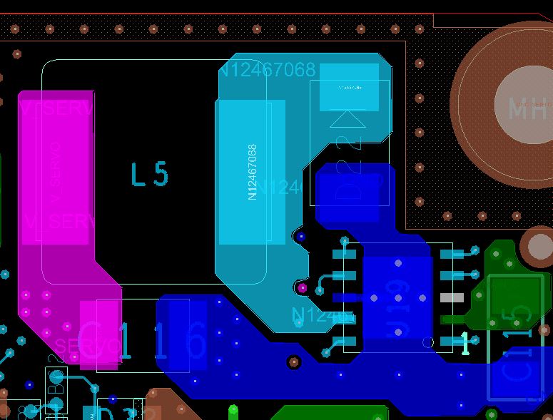
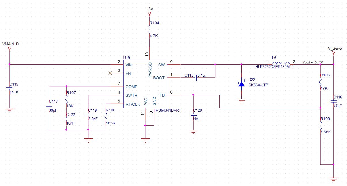
I'm using TPS54341 in my design (attached below) based on WEBENCH simulation I've made (40V input maximum, 2.5A maximum output and 5.7V out).

I'm failing RE102 test (30MHz to 200MHz) due to noise that's generated from the switching of the DCDC.

I've seen that the Vswitch (voltage between SW pin and inductor) is the cause to my EMI problem that's generated around 160MHz.

Is there a possibility to change the resistors/capacitors of the COMP, SS/TR and RT/CLK to reduce switching noise of the DCDC?

How changing the Fsw will affect the rise time (SW pin voltage rise time)?

If not, is there a pin compatible replacement that will give better results? Maybe a device with spread spectrum option?

Best regards,

Igal

  • As I increase the output load, the interference also rises (as expected).

    Attached layout as well.

  • Igal,

    Quick Tests:

    • Try rotating the inductor 180 degrees. Inductors are wound from the inside-out. If the SW node is connected to the pad connected to the center of the windings, the outer windings will shield the noisy center windings. It's silly but it's a quick check.
    • Add a 10-ohm Rboot in series with Cboot (C113). This extends the slew of your high-side FET.

    Suggestions:

    • Add a 1uF and 0.1uF cap close to the VIN pin.
    • Add an LC filter on the input

    Unfortunately we do not have any pin-for-pin replacement with Spread Spectrum.

    -Sam

  • Hi Sam,

    Thank you for your quick and professional reply.

    I tried the following:

    1. Added small value capacitors close to VIN - Didn't help.

    2. LC filter - I already have input common mode chock with feed through capacitors before the DCDC.

    3. I tried adding Rboot of 10 ohm in series with Cboot and it did help:

    It reduced the spectral noise at about 6-8dB and reduced the overshoot from about 3.3V to 1.8V.

    I'd like to reduce the overshoot even more using Rboot and Cboot combinations, but I don't know what's my maximum limit of this method. I'm guessing that the minimal on time will some how limit my efforts.

    I'd also like to test the possibility of adding a snubber circuit (resistor-capacitor network from SW pin to GND) to reduce the overshoot even more, but again, I don't know what's the maximum limit of this method - probably maximal dissipated power on this network.

    Best regards,

    Igal 


  • Igal,

    You can definitely try different values of Rboot. And a snubber is a good idea. This Application Report has lots of great info for selecting and optimizing boot resistors and snubbers.

    If you do another layout spin, you could also reduce the area of your switch node and surround it with a GND plane. That may also help a bit.

    -Sam