This thread has been locked.
If you have a related question, please click the "Ask a related question" button in the top right corner. The newly created question will be automatically linked to this question.
Hello.
LM5101 finds problems in testing, and TI needs to help confirm.
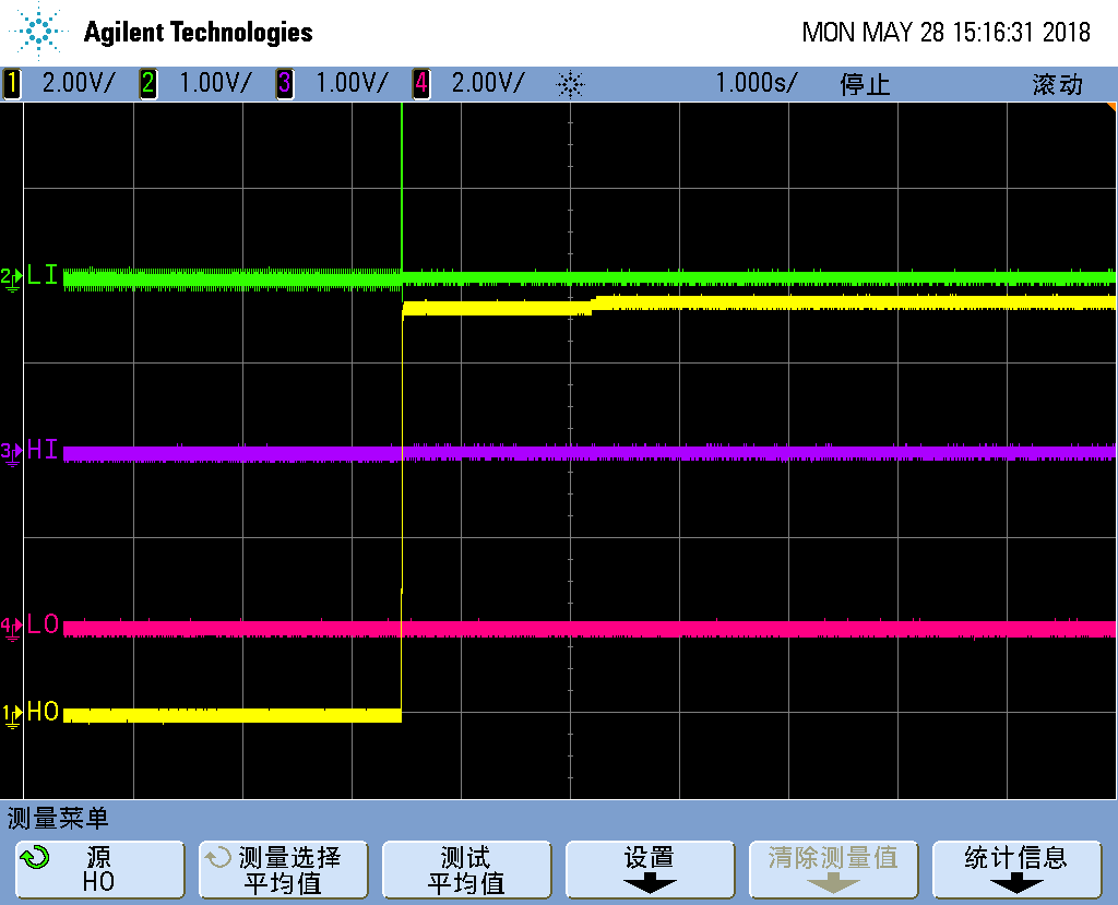
When LM5101 is used, when the LM5101 5pin(HI) and 6pin(LI) level are low, the 3pin(HO) level output is high. The actual test is not the same as Datasheet.
LM5101 The input and output logic table is as follows
Best Regards
Leon
文晔集团
广东省深圳市南山区高新中三道9号环球数码大厦12楼
Mobile:(86)159 8985 2994
Tel:(86)755-26743880 Ext:6643
Fax:(86)755-26743990
Hi, Jeff
Thank you for your support.
The LM5101 circuit diagram
LM5101 test conditions are as follows:
Input=(10~80)V, Output=(0~80)V, LM5101 VDD=12V
Describe.: LM5101(5&6) pin is set to low level. Test LM5101 Pin3 (HO) is high. Test result cannot match logic table.
Verification method:
System board test: when MCU PWM output is set to low level. LM5101 (5& 6) pin is low level. Test LM5101 Pin3 (HO) is high as attached shows.
Signal IC test: LM5101(5&6) pin short circuit to GND. LM5101 Pin3 (HO) is high as attached shows
For your questions, replied as below.
Can I see a scope plot of HI,HO,HS during this issue? ------as system board setup shows.
Can I see a the gate drive portion of the sch and operating conditions? ------drive portion is as LM5101 SCH
what do you mean your test is not the same as the datasheet? ------LM5101(5&6) pin is set to low level. Test LM5101 Pin3 (HO) is high. Test result cannot match logic table.
can you resend the input and output logic table? I cant see it.---logic table is as above.
Best Regards
Leon
文晔集团
广东省深圳市南山区高新中三道9号环球数码大厦12楼
Mobile:(86)159 8985 2994
Tel:(86)755-26743880 Ext:6643
Fax:(86)755-26743990
Hi, Jeff
Thank your for your support.
LM5101 circuit diagram is as follows:
LM5101 Input/ Output Logic Table
Sorry, I did not test the HS pin waveform.
我在客户公司测试LM5101A , 测试HI, LI, HO, LO的波形。
I tested LM5101A in client company to test the waveform of HI, LI, HO and LO.
The waveforms of HI, LI, HO, and LO are as follows:
Signal IC set up.
Test waveform of system board
Best Regards
Leon
文晔集团
广东省深圳市南山区高新中三道9号环球数码大厦12楼
Mobile:(86)159 8985 2994
Tel:(86)755-26743880 Ext:6643
Fax:(86)755-26743990
Hi Leon,
Thanks for your update. I notice that VCC goes to 25V. The recommended operating conditions for LM510x is up to 14V. Exceeding this limit can damage the part, in this case it seems to be damaging the highside output for some reason, maybe inrush the lowside output is not damaged.
Thanks,