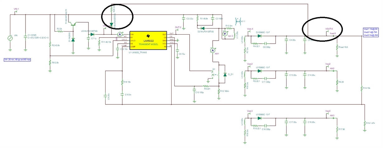
Is it ok to connect Vout:6 (secondary output ) to vin pin ? Is it recommended ?
This thread has been locked.
If you have a related question, please click the "Ask a related question" button in the top right corner. The newly created question will be automatically linked to this question.
GD calcs_27th may.xlsxThank you .
**Here iam planning not to use auxiliary winding to power up VCC because of two reasons
1. i am doing a planar transformer design,so i am exploring other ways to power up vcc so as to save space in PCB by not using auxiliary winding.
2. My Nprim :2 and Nsec is 1.
If iam using Auxiliary winding with Naux/Nsec as 1/1 then 14 V will be seen on Vcc pin which is not recommended as per datasheet of LM5022.
If i set Vaux to 9V then i would get a turn ratio of Vaux/Vsec as 9V/14V =.642 .Here i dont know how to implement this half turn ratio .(Here , i can use a different AL value in ELP22 core set to
increase the Nprimary turns and get more Nsec turns to get Vaux as 9V ,but these more turns would occupy space in PCB.
The next option is connect Vout1 (14V) directly through a diode to VCC of LM5022. I understand that VCC can withstand only 14V .So, i cannot use this option.
Here , i am checking if the requirement of Vout1 14V can be reduced to 9V.
The next option is connecting Vout1 directly to Vin pin through a diode ( as i have shared picture earlier).
while exploring this option i understood that the Tj can go to 53C at Tamb of 25C and Tj of 153C if Tamb is 125C.
( i did Pd calculations based on Tj=Tamb+((vin- Vcc)*(iCCmax+Dmax*Gate pulse current occuring due to switching of Primary switch *percentage of rise time of Gate current in the Ton pulse)*Rth(j-a)).
Here i took Vin =13.5 and Vcc =7.5V ). From this analysis i understood the HV preregultor will be under stress and Tj will go to 150+ when Tamb is 125C. so ,this option is risky at higher temperatures,although Tj @ Ta is 53C only.
Please see the attached calcs sheet.
Here , i request you to please let me know your opinion about Vin option and Have you used Vin ( connecting Vout1 to Vin) in any one of your designs to provide supply to LM5022 in steady state conditions?
I need your help.
Thank you Very much Youhao.
I will try out this option. In this option, I think T1 will be in active region always and power dissipation will be more when Vin is 60V (60V from VIn-11v from zener Z1-0.7V from T1 base to emitter). Selecting a very good Pass transistor with low Rth and High Pd will solve the problem.
Also , iam looking at an option of connecting Vout:6 (secondary winding ) in series with a Zener of 3V, diode and connect it to VCC of LM5022 so that VCC can see (14V-3V-0.7V =10.3V). The power loss in Zener could be 3V*36mA =108W (max) .36mA is the ICC ext limit of LM5022.
I will which option is feasible in terms of Power dissipation and cost.
Best Regards
Hafeez