


Dear TI,
Below is the load switch circuit. (Please refer to the external pin reference because the IC internal circuit is wrong.)
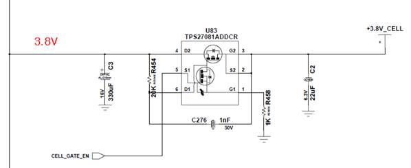
The input is (4pin) 3.8V and the ON/OFF (5pin) is OFF state Low (0V). (6pin also 3.8V)
In this state, 1.15V is output as the output pin (2,3pin).
I am asking TI to confirm that the input and output are not completely blocked.
thanks,
TS
