This thread has been locked.

If you have a related question, please click the "Ask a related question" button in the top right corner. The newly created question will be automatically linked to this question.

BQ25703A: bq25703a VBUS

Part Number: BQ25703A

Hi

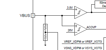
1. could you help check the resister divider value of Vbus pin ? we want to know the resistor value range of VBUS to VIN ? 

2. If I want to turn off  the PMos between VSYS TO VBAT, which regester can I use to control BATDRV pin output  status during charge mode ?

  • 1. I cannot check the resister divider value because I don't have any reason to check it and share the internal circuit design to public. Would you let me know why do you want to know the resistor value range?
    2. During charge, you can set charge option 0 register "inhibit bit" to "1" or you can set charge current register to "0" to disable charger (turn off BATFET).
  • hi wang
    ==>1. my customer want to use this pin to decrease the VBUS drop time, to decrease the time charge mode change to OTG mode. now, customer use 10ohm pull up to Vin, but the resister demage when short Vbus to GND. but change the resister to 1k, BQ25703A can not charge, and we research in datasheet, we didn't find vbus current spec. description. If you can not share the resister divider value, could you help check the pull up resister value range or the Ivbus spec. (between VIN to VBUS)
  • The internal VBus resistor divider should be much higher than 1kohm. You can use quiescent current as reference. But, VBUS is also REGN LDO's input. If you put 1k series resistor, it will have too much drop on that 1k resistor.

    To speed up the transition time from forward mode to OTG mode, they can try to set a lower Vindpm setting if possible.

  • Hi Wang
    To make the 25703A running at the discharge mode: below is the condition which the system need to meet.
    According to 8.3.3 USB On-The-Go (OTG):

    • VBUS is below VVBUS_UVLO

    our system is a DC UPS and the DC output can not interrupt, we also integrated a AC/DC inside, when AC mains ok, the AC/DC will provide the Vdc and 25703 will change the Battery, while when the AC loss, we need the 25703 to running at OTG mode. we need to add one resisitor between the voltage Bus and VBUS pin1 of the 25703,then to pull down to lower when AC loss, to create a treat single to meet the condition of: VBUS is below VVBUS_UVLO.
    if we insert a big resistor before the Pin1, there 25703 can not running stable.
    pls check it and give us more suggestion how to get the design done.

    David
  • David,

    VBUS is also REGN LDO's input. If you put a high series resistor, it will have too much drop for normal application. BQ25703A cannot support UPS application alone. Please let me know if you can make it work.
  • Hi Wang, It seems we can make it works, but need to check more detail with you, where is your location, Can I call you? if yes, pl's mail your number to my 1009307772@qq.com, BR, David
  • Hi Wang
    In the spec page 3: which said, In the absence of an input source, the bq25703A supports On-the-Go (OTG) function from 1- to 4-cell battery to generate 4.48 V to 20.8 V on VBUS. During OTG mode, the charger regulates output voltage and output current.
    My understanding is it can work as the UPS when AC interrupt if combined with the right setup according the 8.3.3. am I Right?

    The holdup time of the AC/DC converter is very long, can be 40~50ms.
    the system also has AC absence detect circuit, when the AC loss, the system CPU( MSP430 ) will setup the 25703 according to 8.3.3. so we have to use a circuit to cheat the 25703 to make the Vbus to lower than the VVBUS_UVLO(2.2~2.6)V

    I saw the LDO input source can be VBUS and VSYS at page 5, 6-V linear regulator output supplied from VBUS or VSYS, can you provide more detailed internal circuit to show how the VSYS or VBUS inputs to the LDO? if we use external circuit to pull the Vbus below the VVBUS_UVLO. does the LDO will also stop working and the 5703 will shut off?
  • David,

    To enable BQ25703A OTG, CHRG_OK has to be low. So, VBUS has to below 3.2V. If you have a circuit to cheat BQ25703A VBUS voltage and hold the system longer enough, you may make it work.

    VSYS and VBUS have a diode OR input to the LDO. Which one has the high voltage, it will power up the LDO. If you pull down VBUS and disable the low power mode from charge option 0, the LDO can keep active.