This thread has been locked.

If you have a related question, please click the "Ask a related question" button in the top right corner. The newly created question will be automatically linked to this question.

BQ25700A: BQ25700Using problem

Part Number: BQ25700A
Other Parts Discussed in Thread: BQ25700, CSD17551Q3A

Hi all,

one of my customer met a problem when using BQ25700 in their design, and the problem shows as below:

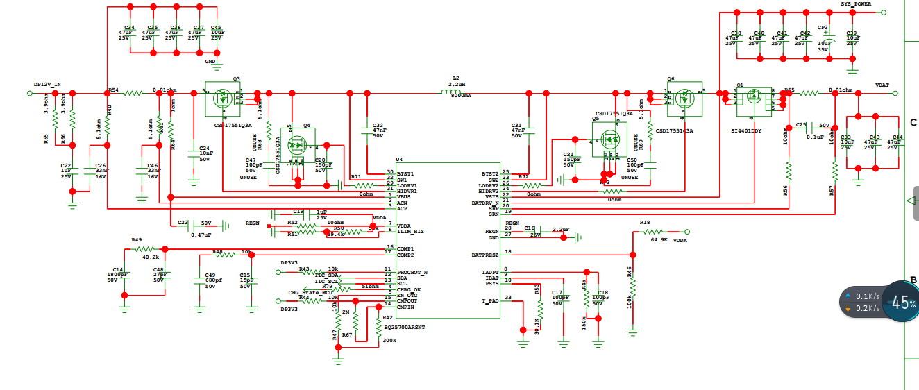
The copper in the inductor and inductor range  generate heat seriously! According to the preliminary testing,the temperature can reach to 60℃ work for 30 minutes.my charging current is 1.3A,the inductor value is 2.2uH.The schematic is as below:

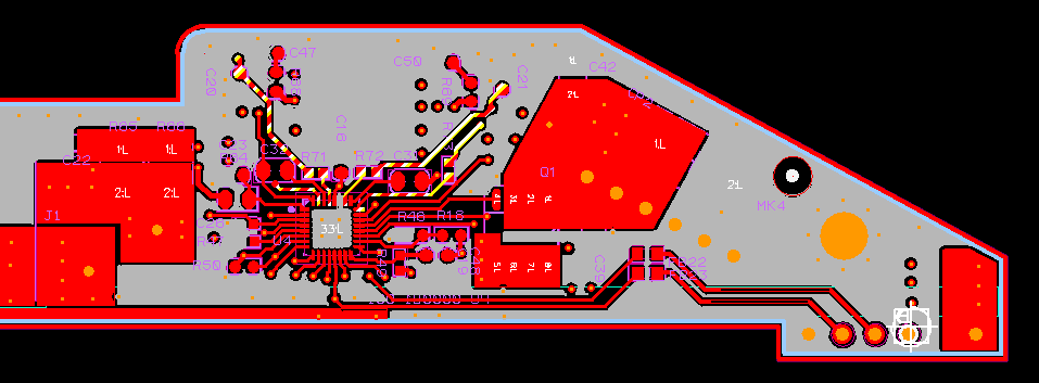
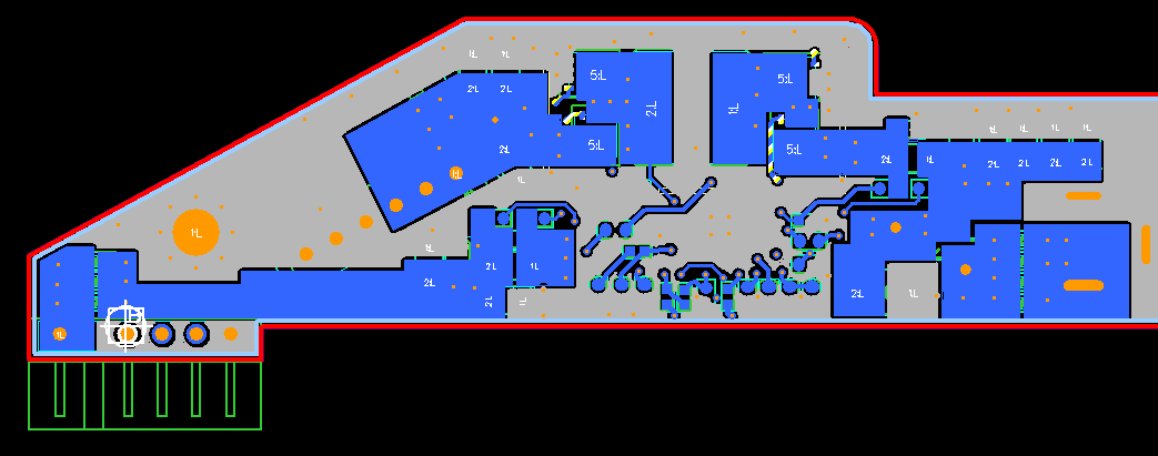
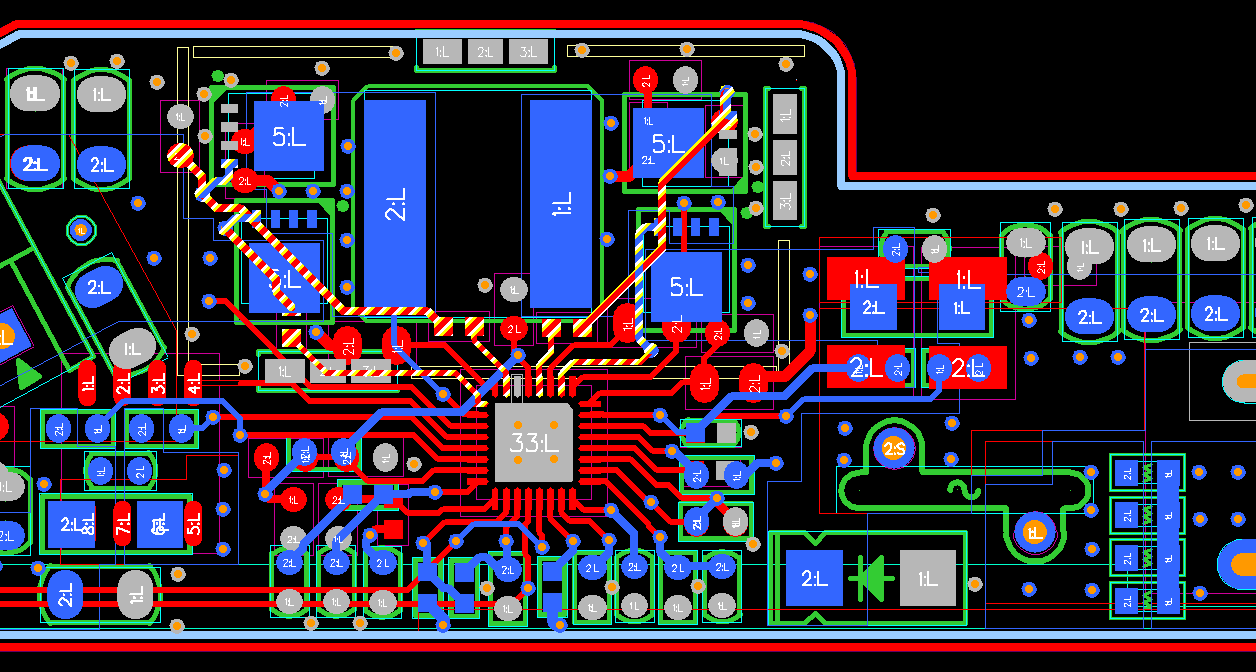
The PCB design is based on the BQ25700EVM, and the trace width is 80mil.could you help me to locate the caouse of heat generation?

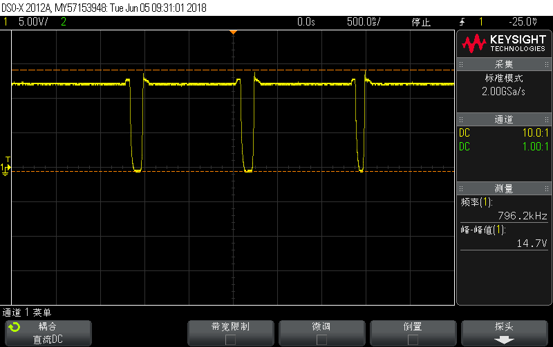
In addition, Why is the switching signal waveform not a square wave?

looking forward to your repply! Many thanks!!!

  • Hello,

    Please help me check the efficiency when it reaches to 60℃ with 1.3A charging current.
    Does the efficiency make sense when you compare it with the datasheet efficiency curve?
  • Hi,

        I have checked the efficiency of my design with an electronic load. The E-load is connected to the VSYS. I set the E-load current from 0.1 A to 1.5A(0.1A per step), and measure the adapter current with an universal meter. The results are as below. Although the core temperature is only about 45℃ (not charging),the efficiency doesn't make sense.Please help me locate the caouse of  heat  generation,and if  you need to know more details,you can email zhangyan@kingrich.com.cn.Thanks a lot.

    电子负载电流(A) 适配器输入电流(A) MCU消耗电流 芯片效率 板卡上损耗(W) 备注
    0.1 0.141 0.03 0.900900901 0.231 电源适配器输入12V,VSYS输出到电子负载的电压也为12V
    0.2 0.246 0.03 0.925925926 0.291
    0.3 0.357 0.03 0.917431193 0.423
    0.4 0.463 0.03 0.923787529 0.495
    0.5 0.583 0.03 0.904159132 0.735
    0.6 0.685 0.03 0.916030534 0.759
    0.7 0.791 0.03 0.919842313 0.831
    0.8 0.903 0.03 0.916380298 0.975
    0.9 1.015 0.03 0.913705584 1.119
    1 1.125 0.03 0.913242009 1.239
    1.1 1.237 0.03 0.911350456 1.383
    1.2 1.354 0.03 0.906344411 1.587
    1.3 1.473 0.03 0.900900901 1.815
    1.4 1.593 0.03 0.895713372 2.055
    1.5 1.714 0.03 0.890736342 2.307

    Best regards,

    Zhang Yan.

  • Yan,

    91% efficiency with 12Vin and 12Vsys is low.

    R45 should be 137kohm for 2.2uH inductor, not 150kHz. The IADPT pin resistor indicates the inductor value.

    Do you measure SW1 or SW2?

    Can you zoom out the switching node waveform? I want to know it is PFM or PWM.

    Can you also zoom in the switching node to find falling and rising edge timing with 1.3A load? I hope the falling time and  rising time can be less than 20ns.

    For the same condition, what is the EVM efficiency?

  • Li

       I have measured the EVM(BQ25700EVM-732) efficiency under the same condition(VSYS 12V, E-load 0.1A to 1.5A).The results are as below.

       I have also captured the switching node waveform of both the EVM and my layout. Results are in the file inserted. But I have no idea if you can download the file. According to the waveform,the rising or falling edge time of my layout doubled(or even worse) comparing with the EVM. Besides,the SW2\LODRV2\HIDRV2 node waveform is not square wave.

       Thanks for the advice. I have already changed the R45 to 137K. Looking forward to your reply.

    电子负载电流(A) 适配器输入电流(A) MCU消耗电流 电源效率 板卡上损耗(W) 备注
    0.1 0.111 0 0.900900901 0.132 电源适配器输入12V,VSYS输出到电子负载的电压也为12V
    0.2 0.216 0 0.925925926 0.192
    0.3 0.324 0 0.925925926 0.288
    0.4 0.43 0 0.930232558 0.36
    0.5 0.532 0 0.939849624 0.384
    0.6 0.645 0 0.930232558 0.54
    0.7 0.756 0 0.925925926 0.672
    0.8 0.869 0 0.920598389 0.828
    0.9 0.975 0 0.923076923 0.9
    1 1.086 0 0.920810313 1.032
    1.1 1.198 0 0.918196995 1.176
    1.2 1.31 0 0.916030534 1.32
    1.3 1.425 0 0.912280702 1.5
    1.4 1.532 0 0.91383812 1.584
    1.5 1.648 0 0.910194175 1.776

    波形对比.docx

    Best regards,

    Zhang Yan

    signal
    BQ25700EVM-732
    My layout
    SW1
    SW2
    LODRV1
    LODRV2
    HIDRV2
  • Yan,

    The switching waveforms are slow from your board. That could cause the efficiency low. For such small current application, we may select a lower Cg with 20mohm Rds_on FET to improve the efficiency.
  • Li,

    I choose the same NMOS whitch is used on the EVM , CSD17551Q3A. Both the Cg(Qg?)and the Rds_on are very low.

    The highlighted lines are the switch node signal on my board(the resistances in series with the switching node signal are 0 ohm.), as shown in the pictures below. Does my layout have such great influence on the switching node signal?What else factors could have influence on the rising\falling edge of  the signal?

    Thanks! Looking forward to your reply.

    Best regards,

    Zhang Yan

  • Yan,

    Is it 2 layer board? Actually, I couldn't tell anything wrong on the layout. I used 4 layer board to do the EVM. It is hard to use 4 layer layout experience to guide 2 layer board layout.