Hello Friends,
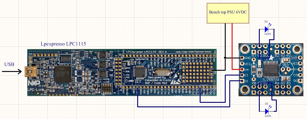
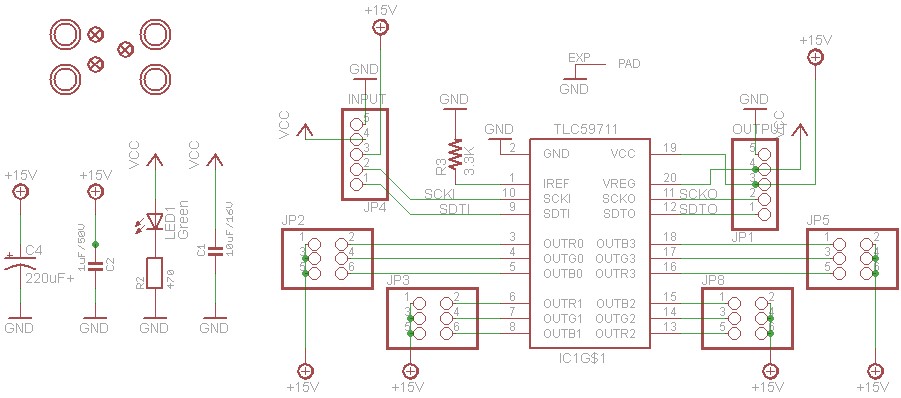
I am using TLC57911 based board (learn.adafruit.com/.../12683) with LPC based eval kit (Lpcxpresso LPC1115). I am using bit bang to generate the SPI (MOSI and CLK).
I took reference of the following code:
- 3113.TLC5971.cTLC5971.h (From: https://e2e.ti.com/support/power_management/led_driver/f/192/t/653874?tisearch=e2e-sitesearch&keymatch=TLC59711)
- Adafruit TLC57911 library (https://github.com/adafruit/Adafruit_TLC59711/archive/master.zip
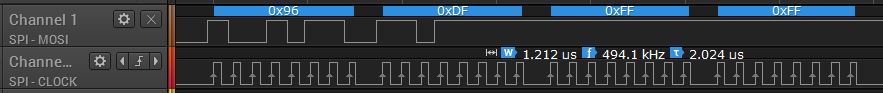
It seems the pulses generated from MOSI and CLK are as per the code can be seen on the logic analyzer but somehow still not able to get the Led's glowing.
Code Snipp:
#include <stdbool.h>
#include <stdint.h>
#include <string.h>
#include <stdlib.h>
#include "LPC11xx.h"
#include "lpc_types.h"
#include "pin_define.h"

#define BUFFER_SIZE (24)

void SPI0_write(uint32_t byte)
{
	uint32_t b = 0x80;

	for (; b!=0; b>>=1) {
		PIN_22_LOW; // Clock
		if (byte & b)
			PIN_28_HIGH; //Data
		else
			PIN_28_LOW;  //Data
		PIN_22_HIGH; // Clock
	}
	PIN_22_LOW;
}

int main(void)
{
    BSP_Initialise();
     Timer_Initialise(LPC_CORE_CLOCKSPEED_HZ, SYSTICK_IRQ_PRIORITY);
    static uint8_t Tx_Buf[BUFFER_SIZE];
    uint16_t i, j=0;

	// Set all leds to around 25% brightness
    for (i = 0; i < BUFFER_SIZE; i++) {
        Tx_Buf[i++] = 16000 >> 8;
        Tx_Buf[i] = 16000;
    }

    uint32_t command;
    // Magic word for write
    command = 0x25;
    command <<= 5;
    //OUTTMG = 1, EXTGCK = 0, TMGRST = 1, DSPRPT = 1, BLANK = 0 -> 0x16
    command |= 0x16;
    command <<= 7;
    command |= 0x7F;
    command <<= 7;
    command |= 0x7F;
    command <<= 7;
    command |= 0x7F;

	while (1)
    {
        SPI0_write(command >> 24);
        SPI0_write(command >> 16);
        SPI0_write(command >> 8);
        SPI0_write(command);

        for (j = 0;j < BUFFER_SIZE; j++) {
            SPI0_write(Tx_Buf[j]);
        }
        Timer_Delay_Micro(5);
    }
    return 0;
}
Snapshot of the Logic analyser connected to the the input CI and DI (Clock Input/ Data Input) with 3.3V on the TLC57911 based board.
First Four Bytes:
First 14 Bytes (as cannot get in single screenshot):

Second 14 Bytes:

H/W Connection between LPC and TLC57911:
| LPC1115 | TLC57911 based board |
| MOSI | DI (Data Input) |
| SCK | CI (Clock Input) |
External 6V is given to V+ pin on TLC57911 board
Common GND is used: External GND, LPC1115 GND and TLC57911 board GND are interconnected.
Can anyone please hint/tip why it's not working as expected?
Please share if you need any further information.
Cheers,
Ankur