This thread has been locked.

If you have a related question, please click the "Ask a related question" button in the top right corner. The newly created question will be automatically linked to this question.

TPS65131-Q1: TPS65131-Q1 suggestion Vref Cap value

Part Number: TPS65131-Q1
Other Parts Discussed in Thread: TPS65131

Hi, Brigitte

For this question :We saw similar waveforms at other customers and the problem was layout. Please check with the customer if there might be noise coupling into the FBN node. Even if at the moment the problem seems to be solved by changing the capacitor, if the layout of FBN is in a noisy area, it could come back later in mass production.
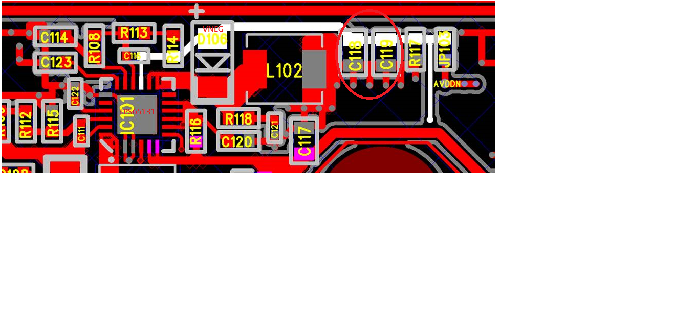
below as schematic:

123fca1 DC電路圖.pdf

and also we saw client layout  FBN was not loop output cap, it`s look like coupling noise issue.


and Could you explain this phenomenon?  why we fine tune R and C value can fixed issue.

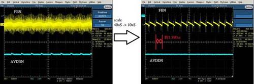
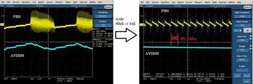
as below was client change R and C test result.

C116(pF)

R108(K ohm)

R113+R114(K ohm)

C116*(R113+R114)

AVDDN

FBN

2

15.4

82.6

165.2

no Ripple,voltage level is correct(-6.5V)

stable

2

47.5

255

510

no Ripple,voltage level is correct(-6.5V)

stable

22

15.4

82.6

1817.2

have Ripple(-6.0~-8.0)

sometime unstable

8

15.4

255

2040

have Ripple(-6.0~-8.0)

sometime unstable

22

47.5

255

5610

no Ripple,voltage level is wrong(-9V)

unstable

 A. C116*(R113+R114)if  increase R and C Value (almost 5610*10-9)FBN was unstableAVDDN was wrong voltage. 


B.C116*(R113+R114) If decrease R and C Value (almost 510*10-9)FBN was stable,AVDDN voltage was correct.

C.C116*(R113+R114) almost 2040*10-9時FBN sometime unsaable,AVDDN have Ripple


if any, Please advise me.


Thanks,


Best regards,


Lawrence.


  • Hello Lawrence,

    As the feedback divider is connected to the diode and not to the output capacitors, all noise coming from the switching activity is directly going into the feedback node. If the feedback node would be connected to the output capacitors, most of the noise would be filtered by the caps and less noise would be coupled into the feedback node.
    Not optimized layout is the biggest concern in power supplies, especially on the noise sensitive node (because high impedance). In TPS65131 the FBx and Cx nodes have to be prevented from noise because noise coupled into the regulation loop can cause voltage shift, instability, increased ripple and even no output at all.
    Playing with the external components can reduce the noise coupling, but normally a layout issue will not be solved, just masked by such activities.

    Best regards,
    Brigitte
  • Hi, Brigitte


    i Got it. Thanks!


    Playing with the external components can reduce the noise coupling, but normally a layout issue will not be solved, just masked by such activities.

    external components can reduce the noise coupling, coulde you can share ?

    If any suggestion, Please advise me.

    Thanks,

    Best regards,

    Lawrence.

  • Hello Lawrence,

    The customer already reduced the noise coupling with changing the external components, because he made the board work, but as said this is not a recommended solution for production.

    Best regards,
    Brigitte