This thread has been locked.

If you have a related question, please click the "Ask a related question" button in the top right corner. The newly created question will be automatically linked to this question.

TPS62175: En 61000-4-5 surge protection

Part Number: TPS62175

HI,

I used tps62175 Step-Down Converter to make the DC-DC conversion on my board, from 24V to 5V. It works, schematic:

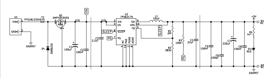
Now I faced with device certification. I failed En 61000-4-5 test for Class A (R=2 ohm and signal shape 8/20 us). Actually, I passed +500V impulse. On -500V impulse device failed, tps62175 blow up. I suppose that high negative voltage appears at tps62175 inputs.

I used unidirectional TVS diode SMBJ24. Does bidirectional diode resolve my problem?

Any suggestions will be helpful, thanks.
Apologies, If I use the wrong forum.

  • Hi,

    Could you please describe in more details how/where you apply the +500V and -500V?
    You say the device blows up after the -500V pulse. Can you check which pins are damaged/shorted?
    Does your setup allow you to measure the waveform at the device input during the testing? If yes, could you provide this?

    Thanks.
  • Hi,

    I don't have any measured results. On the image below you can see that input pins are damaged, pin 2 and 3:

    I suppose that my diode, SMBJ24, stopped to work while -500V was applied. During this period current can go up to 250A which is too much for this diode. And as result -500V appeared on tps62175 input. Do you agree?

  • Hi,

    Yes, I think you're right. Did you observe that the diode was damaged during the test?
    SMBJ series is limited to 600W. Did you try a comparable diode from the SMCJ (1500W) or SMDJ (3000W) series?
    We would also recommend to try a Schottky diode in parallel to the SMxJ diode (same direction). The Schottky diode would react quicker and help clamp the voltage during the -500V pulse.

    Thanks.
  • Hi YD,

    thanks for the reply.
    Meanwhile, I was in lab and device passed the surge test. Bidirectional SMDJ diode resolves my problem.

    Now I faced with a new problem. Device fails on Immunity to Conducted Disturbances, Induced by Radio Frequency Fields, 6100-4-6 standard. My device, same circuit from my first post here, isn't immune in the range (23-26)MHz. Applied voltage during this test is additional 3V/m.
    I think that this problem can be solved by selecting an appropriate capacitor and place it on DC-DC converter input. To calculate the elimination frequency I used the following equation:
    f = 1 / ( 2*Pi*sqrt(L*C) )

    Do I think well?

    Thanks,
  • Hi Srdjan,

    Good to hear you now passed the surge test.

    Regarding your new problem: yes, I think your reasoning and equation are correct.

    The challenge is here to use the right value for the parasitic inductance, which you could either measure or obtain through parasitic extraction of your PCB.

    Thanks and regards, YD

  • Hi YD,

    Thanks for the reply.

    Yes, parasitic inductance is an open question. For ceramic capacitor I couldn't find information for parasitic ind. in a datasheet, for examples 50nF or 5nF. So I researched and found out that for 0603 package parasitic ind. is 870pH, according to THIS document. Does it make sense?

    Another thing is how many capacitors do I need to eliminate noise in range (23-26)MHz, each capacitor for each +1MHz?

  • Hi YD,

    Thanks for the reply.

    Yes, parasitic inductance is an open question. For ceramic capacitor I couldn't find information for parasitic ind. in a datasheet, for examples 50nF[https://eu.mouser.com/ProductDetail/581-12065C503JAT2A] or 5nF[https://eu.mouser.com/ProductDetail/581-08055C502KAT2A]. So I researched and found out that for 0603 package parasitic ind. is 870pH, according to THIS document [https://www.avx.com/docs/techinfo/CeramicCapacitors/parasitc.pdf]. Does it make sense?

    Another thing is how many capacitors do I need to eliminate noise in range (23-26)MHz, each capacitor for each +1MHz?
  • Hi Srdjan,

    Regarding parasitic inductance: Yes, I think what you found makes sense. Do not forget to take into account the parasitic inductance of the PCB trace as well, which I also expect to be in the ~nH range.

    Regarding capacitors: one capacitor dimensioned around the middle of the frequency band should be enough.

    Altogether it would be advisable to try a few configurations and fine-tune the values by experimentation...

    Thanks and regards, YD