This thread has been locked.

If you have a related question, please click the "Ask a related question" button in the top right corner. The newly created question will be automatically linked to this question.

WEBENCH® Tools/UCC28C42: Custom part numbers?

Part Number: UCC28C42
Other Parts Discussed in Thread: TL431

Tool/software: WEBENCH® Design Tools

Hi,

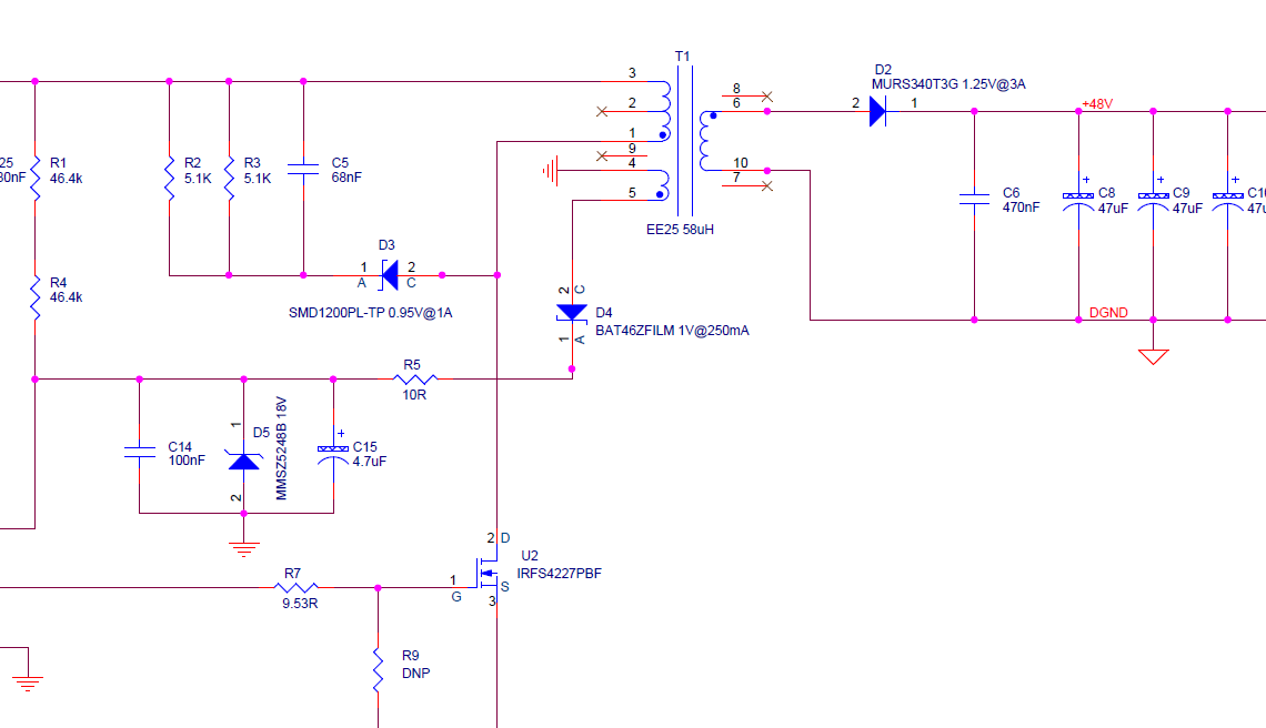
I am designing a DC-DC converter.

Vin (Min) (V): 36
Vin (Max) (V): 75
Vout (Nom) (V): 48
Iout (Max) (A): 1
Output Power (W): 48
Isolated/Non-Isolated: Isolated
Input Type: DC
Topology: Flyback

Webench has generated a schematic for me but, some parts are missing.

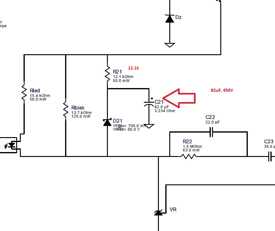
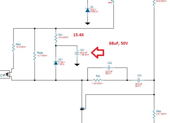
It tells that diodes are custom. How can they be? and why two diodes in parallel? Do we need these diodes? if yes then please suggest an alternate part.

NPN transistor at VREF of UCC28C42 is 2N2222A this is a through-hole and costly part. Is there any alternative to this?

Regards

Vishal Kakade

  • Hi,

    One more thing, how to design an input EMI filter for this design.?

    Regards

    Vishal Kakade

  • Hello Vishal,

    Thank you for your interest in designing with the UCC28C42 PWM controller.

    The Webench design tool is intended to produce a design that will work, based on the input and output information provided, but it is not sophisticated enough to produce an optimal design. Essentially, it solves a series of design equations for each component and tries to match the calculated parameters to a database of parts to select the closest fit. However, the Webench database is relatively limited compared to the inventory of a parts distributor, for example. In some cases, as in the case of the output diodes, there may not be a suitable part available from the database, so the Webench program provides only the parameters necessary so that the user may find an equivalent part that is readily available. I don’t know why the program uses 2 diodes in parallel, unless it did so to minimize losses.

    Similarly, I think a 2N2222A was designated because of a limited set of small-signal transistors in the database. You are not required to use this exact part. An experienced designer knows that every one of the parts in this design have multiple alternatives: either for sources of parts with the exact values, or substitutes with similar values with perhaps some other advantage such as price or availability.
    A surface-mount substitute for the 2N2222 can be an SMD version of the 2N3904 or 2N4400 devices to name a few. I don’t know the actual SMD part numbers off-hand, but an on-line search should turn up several vendors and searching their product line will turn up many possibilities. In this application, the transistor needs minimum ratings of 10V Vceo and a few mA of collector current.

    As for designing an input EMI filter, one must first determine whether such a filter is even necessary based on conducted noise-level specifications that must be met. With a low-voltage DC input, any noise specs are likely to be different than those usually required for an off-line AC application.
    Then the amount of noise generated by the converter must be measured to determine the amount and type (common mode and/or differential mode) noise that needs to be attenuated. Finally, a filter arrangement is selected and values calculated to achieve that level of attenuation. Her is a link to some training in EMI design: training.ti.com/.../understanding-emi-and-mitigating-noise-dcdc-converters input line filter&tisearch=Search-EN-Everything
    This training may contain more information than you need, but it should give you a good overview of what is involved.

    Regards,
    Ulrich
  • Hello Ulrich,

    Thanks for your support. I have one more doubt regarding the transformer as I don't have much experience working with them.

    As per the requirements suggested by webench, I have designed my transformer. 

    Winding

    Start pin

    Finish pin

     Turns

    No of wires.

    Wire size(mm)

    Direction of wdg

    Tape

    (No. of layers)

    Remarks

    W1 Primary first half

    3

    2

    10

    1

    0.40

    C.W

    2


    W2 Auxillary

    5

    4

    06

    1

    0.32

    C. C. W

    2

    Spread wind

    W3 Secondary

    6

    10

    19

    1

    0.40

    C. C. W

    2


    W4 Primary Second half

    2

    1

    09

    1

    0.40

    C.W

    3

    Please tell me which pin no are positive and which are negative. As I am confused with winding direction and dot notation on the transformer.

    Regards

    Vishal Kakade

  • Hello Vishal,

    The dot notation on schematic diagrams of transformers is used to indicate the polarities of each winding with respect to each other. Using dots (other symbols may also be used, but dots are the most common), the voltage polarity of all of the windings can be established when the voltage of one winding is known. The voltages across all of the windings can be either positive or negative at any given time, but those voltages follow the polarity marks.

    It doesn’t matter if the transformer is used in a flyback topology or a forward-mode topology, when a voltage is forced across a winding (such as when the main transistor is turned on and bulk voltage is applied to the primary winding), if the applied voltage is positive at the dotted end of the winding and negative at the non-dotted end, then all the other windings will be positive at their dotted ends. The opposite can also be true: if the applied voltage is negative at the dotted end of the winding and positive at the non-dotted end, then all the other windings will be negative at their dotted ends. It also does not matter if the dots indicate positive or negative voltage as long as they are all of the same polarity, but usually (although not always) a positive voltage is ascribed to the dot.

    The dots are used to indicate winding polarity on paper, for convenient reference. In a physical transformer, the direction of winding construction determines the relative polarities of each winding. Usually, the paper schematic is drawn to indicate the desired circuit function and the physical transformer is constructed to match it. Clockwise and counter-clockwise winding directions with respect to the core are established to obtain the required polarities. They are based on the “right-hand rule” for flux direction with respect to current direction. This rule says that when you curl the fingers of your right hand into a fist and stick your thumb out, current flowing in the direction of your thumb (as in a wire) generates flux around the current in the direction of your fingers. The converse is also true: flux pointing in the direction of your thumb is established by a current flowing around the flux (as in a coil of wire) in the direction of your fingers. If you look at your right-hand thumb pointing at your nose, your fingers are wound in a counter-clockwise direction around your thumb.

    To picture a winding structure more fully, I sometimes draw a vertical core on paper and then overlay each winding along the core. Start with a main winding, such as the primary (for example), and assign the start of the winding to some pin number and the finish of that winding to another pin number. Assign the direction of flux in the core as point up to the top of the sheet for a positive voltage applied to the winding. Lay your hand on the sheet with thumb pointing up in the direction of the flux in the core. Your fingers point in the direction of the wire winding necessary to generate that flux based on a current flowing in that direction. Beginning at the start pin, wind the wire counter-clockwise across the core, going down into the sheet on the right side, coming back under the core and coming up out of the sheet on the left side to complete one turn. Continue with all of the turns needed from the start pin to finish pin for that winding (or winding segment for split windings). All other windings wound in the same direction will have the same polarity as the first winding. Those wound in the opposite direction will have the opposite polarity.

    Following this method with your transformer design, if we arbitrarily assign a dot at “start” pin 3 of W1, then a dot is also placed at “start” pin 2 of W4, since it is wound in the same direction as W1. Since W2 is wound in the other direction, the dot is placed at “finish” pin 4. Similarly, a dot goes to “finish” pin 10 of W3.

    I believe it is good practice to VERIFY that your completed transformer matches your paper design by applying a high frequency sine-wave voltage from a signal generator to one of the windings and checking the other windings for voltages of the expected polarities, appropriately scaled by the expected turns-ratios. Only a 1V (or a few volts) peak is necessary, at a frequency higher than 10kHz (like 50~100kHz) to avoid loading down the signal generator due to low winding impedance, and to avoid saturating the core of very small transformers.

    A treasure-trove of information on magnetics can be found in the TI/Unitrode Magnetics Design Handbook at www.ti.com/.../slup132.pdf , but ironically little is discussed about polarity and winding direction. Some mention of these are made in the reference articles R3, R4 and R6 near the end of the handbook. More reference sources on polarity fundamentals can be found by searching the web for “magnetic dot polarity” or other similar search string.

    Regards,
    Ulrich
  • Hello Ulrich,

    Thanks for your response, As per the info provided by you and from the transformer manufacturer, I have chosen the following polarity please correct me if I am wrong.

    Pin No Function
    3 +input to transformer
    2 NC
    1 -input to transformer
    5 + Output of auxillary
    4 - Output of auxillary
    6 + Output of Secondary
    10 - Output of Secondary

    Please Check my Schematic and Table (Ignore the dot notation in the schematic) for correct connection of polarity. Please note Winding details are same as discussed previously.

    Thanks 

    Vishal Kakade

  • Hello Vishal,

    Your polarity table and the dot notation in the schematic coincide.  I see no problem with it.

    When the primary FET U2 is on, there is +Vbulk at pin 3, and all of the dotted ends will have a negative voltage with respect to the other ends.  When U2 turns off and the core demagnetizes, all of the dotted ends will have positive voltage with respect to the other ends.  This is completely normal and proper for a flyback transformer. 

    Good luck with your design.

    Regards,
    Ulrich

  • Hello Ulrich,

    The current Sense resistor (R-14) suggested is 152.743 mOhm. Which is not a standard part. I am using a 150mohm, 0.33W resistor. Is it okay to use or I need a more power-wattage resistor?

    Regards

    Vishal Kakade

  • Hi Vishal,

    150mohm is a good value to use. The power rating for R14 should be checked by finding the worst-case I^2*R dissipation in it.
    It is my personal preference to determine (or estimate) the worst-case loss in every resistor and choose a part with power rating of double that loss (or use a number of parallel parts to get the double-rating). Sometimes I need to make an engineering judgment of whether to accept something less than double (because of limited time in a worst-case condition, for example), but generally doubling the power has proved to result in reliable operation of resistors.

    Webench should be able to tell you what the power loss in R14 is, and what the rms current in U2 is. Click on the "Op Vals" box (along the top of the Webench window) to find listings of the operating values of all the various components under various operating conditions. If using more than one resistor (parallel or series to get the same net resistance value) the power in each part is the total power divided by the number of resistors (as long as they are all of the same value).

    Regard,
    Ulrich
  • Hello Ulrich,

    I have simulated my design twice for same parameters and getting different results on webench why?

    Input (36-75)

    Output: 48V

    Iout= 1A.

    I have space constraints on my board.First, it is suggesting 82uF, 450V later it is showing 68uF, 50V. Why is this? What is the actual value that is required and what is the function of that capacitor?

    Regards

    Vishal Kakade

  • Hello Vishal,

    The Webench design program is basically a series of design equations that are solved based on the parameters and constraints of the specific controller selected and the input parameters provided by the user. I would expect that if a design was run twice (or any number of times) with exactly the same inputs, it should produce exactly the same outputs. Since you got two different results, I guess that you somehow did not have exactly the same conditions set. Although the 36-75V input and 48V, 1A output is the same, some other subtle parameter may have been changed, such as cost, efficiency or size optimization settings or something like that.

    The purpose of that capacitor C21 (and R21 + D21) is to provide a soft-start rise of the output voltage by slowing down the rise of the TL431 cathode voltage. Like most controllers with this kind of feedback structure, full power is delivered to the output when the opto-coupler current is cut off and minimal power is delivered when the opto current is maximum. At start up, there is no output voltage and no opto current, so full power is delivered to charge up the output cap(s). As Vout increases, some current can begin to flow through Rled and Rbias, into the TL431. Since Vout is still low, its feedback keeps the TL431 off so its cathode voltage wants to stay high and keep the opto off. Soft-start cap C21 counteracts this by pulling the cathode voltage down through D21 and keeping the opto current higher so less power is delivered. The main purpose is to prevent overshoot of Vout at start-up. After start-up, R21 keeps charging C21 higher to the Q1 emitter rail voltage (~20V from Dz) so that D21 can block the C21 capacitance from affecting the TL431 transient response after start-up.

    That said, all of these parts (C21, R21, D21) are flexible, and in fact, completely optional. You may or may not need the soft-start circuit and maybe can eliminate all 3 parts. Test your prototype by removing C21 and observing the start-up response to decide if it is acceptable or not. If soft-start is needed, then the value of C21 can be adjusted to determine how “soft” the start-up should be. Lower values are quicker, so overshoot level can be tailored to minimize C21 value. R21 is just an after-start pullup, so it does not have to be 15.4K (which increases the value of C21 to keep a certain rise time), so I suggest increasing it higher to 47K or 100K or so, to help minimize C21. D21 does not need to be a Schottky diode; it can be a signal diode such as 1N4148-type (or similar, in SMD package). The voltage rating of C21 depends on how high its voltage gets. With 20V at Dz, I think a 25-V rating on C21 is sufficient.

    Webench solves a series of equations for circuit components and “chooses” physical parts to match the calculated component parameters from a database of parts loaded into it. This is a finite database, not nearly as extensive as an electronics distributor might have. For the 68uF cap, it found a 50-V part but for the 82uF cap it could only find a 450-V part in its parts list, so that is what was presented. (In either case, only 25-V is actually needed.) Some minor difference in the initial conditions between the two Webench runs caused it to recommend something higher than 68uF and the next available part that it could find was 82uF/450V. This points out that Webench is not an Artificial Intelligence but a limited program and a good degree of user judgment should be applied to scrutinize each component recommendation for understanding and sanity check. Webench can give a designer a quick short-cut to a suitable circuit solution from only a hand-full of user inputs, but it is the designer’s responsibility to optimize those results for real-world implementation. Meanwhile, TI strives to continually improve the performance of Webench, but given limited resources with increasing breadth of product lines and a bewildering variety of topological design directions, such improvements are incremental and sporadic.

    Regards,
    Ulrich
  • Thank you Ulrich for all you support.

  • Hi Vishal

    Can you try sharing with me the design for which you saw 82 u capacitor, i created the design for this condition


    Input (36-75)

    Output: 48V

    Iout= 1A.

    Ta = 30 C

    Source - DC, and got 68 u caps, multiple times


    you can find the designs here by clicking on top left - My Designs/Projects

    6116.e2e.docx

    For sharing the design you can click on "Share Design" tab and share it with me ( sahilg@ti.com)

    e2e2.docx

    let me know if any question on this, 

    thanks

    sahil