This thread has been locked.

If you have a related question, please click the "Ask a related question" button in the top right corner. The newly created question will be automatically linked to this question.

LM5575-Q1: LM5575-Q1

Part Number: LM5575-Q1

Hello,

We have implemented DC-DC buck converter to down-convert the 48V to 15V. During the Line regulation testing, we found an issue with the output voltage that not being stable for the whole range of voltages.

The schematic is designed for the operating voltage range of 24V -56V with a nominal voltage of 48V and load current of 0.8A. During the verification of the device, for the following test there has been a unintenteded observation made as explained below.

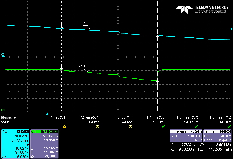
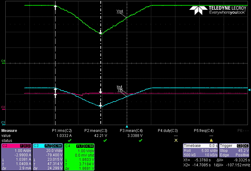
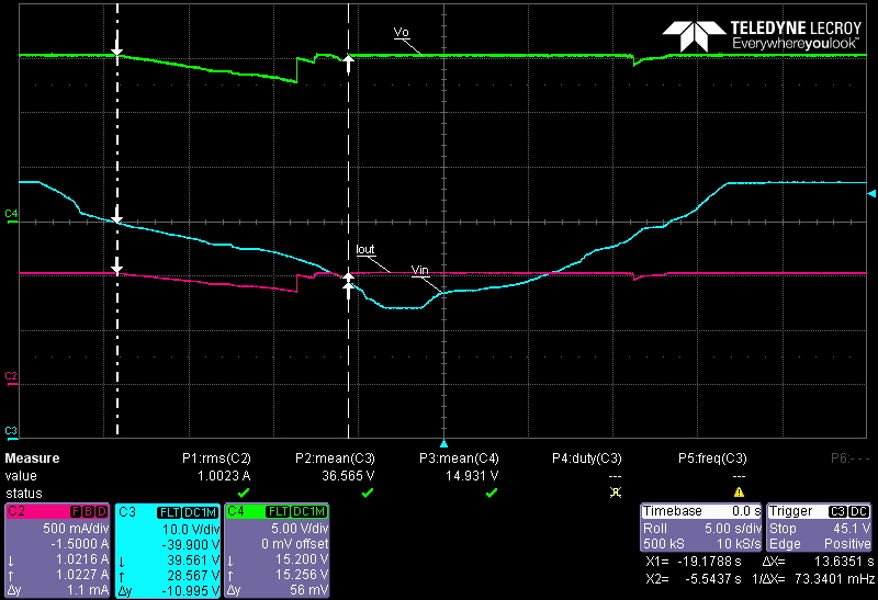
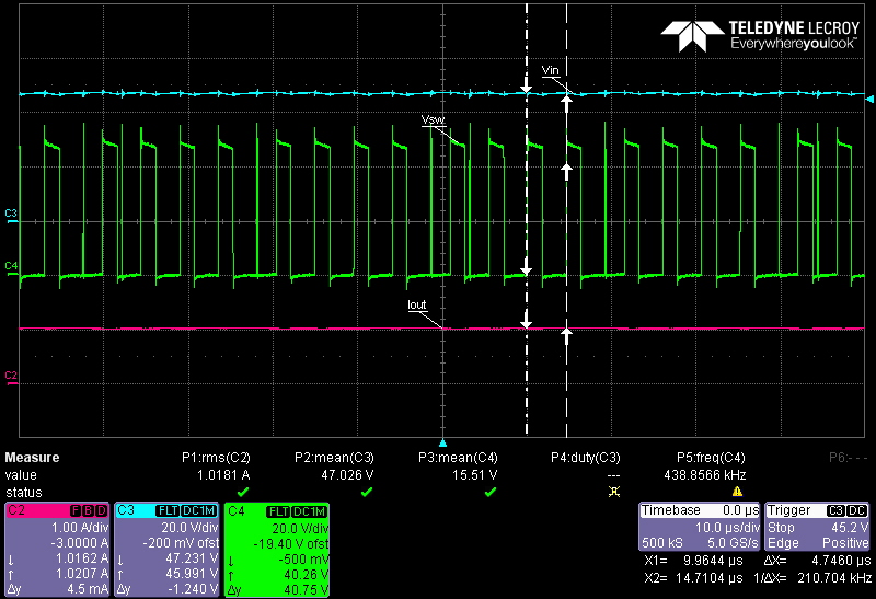
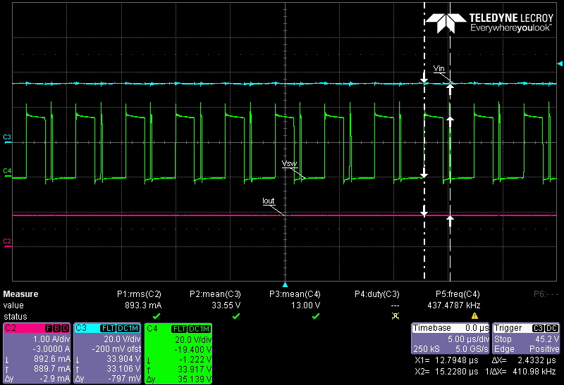
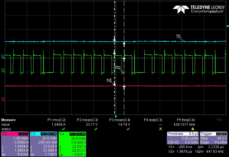
With a load current set to 1A, the input voltage varied from 48V to 25V. During this ramp-down, in the range from 40V to 30V the output voltage was deminishing slowly from 15V to 13V. This was unaccepted from the device.

Could you please look for some reason for this behaviour and get back to me with a feedback?Please revert if you need any additional information on the same.

Thanks.

  • Durgaprasad,

    Please share the schematic and layout.

    1. VOUT diminishes from VIN=40V to 30V. Does it continue to drop when you go down to 24V?

    Please check:
    2. current limit on your supply.
    3. FB with respect to AGND with a scope during these conditions. Does it stay = 1.2V for all VOUTs?
    4. Switch node with respect to PGND during these conditions. Does it look stable? Constant frequency?

    -Sam
  • Ramping down from 30V to 24V the output voltage is going back to 15V and staying there.(We have an under-voltage detection at 24V)

  • Durgaprasad,

    That's interesting that the voltage drops only from VIN=40V to 30V but goes back to normal when going to 24V. That makes me think instability is the issue.

    1.Can you share a scope capture of VIN and VOUT as you ramp the voltage slowly down from 48V to 24V and back up again?

    2. Can you share a layout?

    Please check:
    3. FB with respect to AGND with a scope during these conditions. Does it stay = 1.2V for all VOUTs?
    4. Switch node with respect to PGND during these conditions. Does it look stable? Constant frequency?
  • Sam,

    The FB pin voltage is also going down in this range and i think its very obvious since it is a mere resistor divider.

    Switching frequency is remaining constant during this behaviour of the output.

    Another observation made also indicates that this window for the drop increases with increasing Load current.

    For eg, for 1A its 40V to 30V and for 1.2A its 40V to 24V.

    Layout section:

    First side:

    Second side:

    I suggest you to please reproduce these cases in your lab and let us know if you observe the same.

    Thank you very much in advance.

    -Durgaprasad

  • Durgaprasad,

    Yes, the FB pin is just a resistor divider from VOUT. But sometimes the layout and method of measurement will show an issue on VOUT but FB pin looks fine. If the FB pin looks fine, the IC think's it's doing its job and the solution is to fix what's wrong with the layout. If you're observing that FB is following VOUT exactly (just scaled) then we can think of other possible issues.

    1. It looks like the layout pictures didn't attach. Can you please try again?

    Please share:
    2. A scope shot of FB with respect to AGND during your slow VIN ramp down.
    3. Switch node with respect to PGND during these conditions. Does it look stable? Constant frequency?
  •  Sam,

    From what i have observed on the scope the FB pin voltage is properly following the VOUT.

    2.Also FB ramp down is similar to Vout ramp down.

    3.Switch node frequency when checked it is found to be stable at 438kHz.

  • Durgaprasad,

    Please also attach the back-side layout.

    1. Why did you add R119? This should be a short from the DAP/SUBS to PGND
    2. Why did you add R121? This should be a short from OUT to the output voltage.
    3. What is the voltage on SD during this ramp down?
    4. Please attach a scope shot of VIN ramping back up, please. I'd like to see if VOUT is consistent between ramp up and down.
    5. Please attach a scope shot of the SW node at VIN = 48V. Then attach more at any input voltage down to 24V if the switch node changes in shape, frequency, or consistency (wobbling duty cycle).
  • Sam,

    Layout other side:

    1 and 2 : these values are from one of reference application we considered.I also made check by replacing these resistors with zero Ohm resistors. This is not helping the situation.

    3. Since the SD voltage is fed through the resistor divider from Vin, it is following the Vin itself.

    4. Below is the image you find for Vin ramp-down from 48V till 25V and ramp-up again from 25V-48V. The Vout drop is observed only during the ramp-down and not during the ramp-up.

    5. Below you find the waveforms of the Vsd pin for various input voltages.

    a. Vsw @ Vin = 48V  (No fault)

    b. Vsw @ Vin= 35V (Faulty range: Vout is less than 15V)

    c. Vsw @ Vin= 25V (No fault)

    I checked also the inductor current to check if the ripple current is hitting the over-current limit of 2.1A, but i did not find anything like that. Please cross-check at your lab and let me know if you find any solution for the issue..

    Thanks,

    Dp

  • Dp,

    Thank you for sharing the back-side layout. It looks like the power side of the layout is cut off on the right.

    1 and 2. If this is a TI design, please send me the link.

    3. Okay

    4. Interesting that it's happening at ramp down but not ramp up. Seems like something is latching somewhere. It would be interesting to ramp up and down to see what voltage causes the latch.

    5. The switch node on all of those plots looks irregular. SW should be a constant frequency square wave with a constant duty cycle (at steady state). This design has issues with stability and it's most likely caused by the layout.

    Here are layout guidelines for your design:

    A) It's best practice to keep the IC, inductor, diode, boot cap/res, CIN and COUT on the same side of the board.

    B) The traces to and from D102 are too small. This should be a thick trace.

    C) D102 is a 1A diode. You may want more margin for your 1A circuit.

    D)  The inductor is far away from the converter. Place it close to the converter and use a thick trace.

    E) The inductor has a long trace to the output caps. These caps should be placed very close the inductor and should have a thicker trace.

    F) The VOUT signal to the feedback divider is connected part-way down the trace from VOUT to the load. This should be connected to VOUT at the capacitors.

    G) Make sure the DAP/SUBS/Exposed pad is connected to the GND plane for heat dissipation.

    There may be more but it's tough to tell with the information I have. Check the datasheet for layout recommendations for your next board spin.

    -Sam

  • Sam,

    This was not a TI reference design.

    I am quite sure we have some flaws in our layout design. This was also because of the space/height constrains we were limited with. I would try to strictly consider your suggestions in our consequent sample.

    Could you please share with me the typical waveforms for Vsw,Vfb,Vbst during the normal operation and during the ramp-up and ramp-down? It would really help me to refer them for my design.

    Also if possible, could you please send us one evaluation kit which can be used as a standard reference?

    -Dp

  • Dp,

    You can find the evaluation module on store.ti.com at this link.

    Find below waveforms for 5VOUT, 1AOUT at VIN=10V, 24V, 48V, 48V (zoomed in)

  •  Sam,

    The issue has been resolved. It was a simple mistake which both of us failed to observe. :(

    The Capacitor at RAMP pin was too big (220nF). The recommended value is 50-2000pF. And for my design it should be 470pF.

    Now everything works fine.

  • Dp,

    Oh, yes, that makes a lot of sense. I'm glad it works now and thank you for letting me know!

    -Sam