This thread has been locked.

If you have a related question, please click the "Ask a related question" button in the top right corner. The newly created question will be automatically linked to this question.

LM5104: To work as a switch, not with PWM

Part Number: LM5104

Hi !

I am as Rodrigo working on a prototype based on the LM5104 working as a switch. The purpose of this montage is to turn on/off a DC voltage (VCC2) going from 1,25 to 7V with a standard 3V3 logic command, knowing that it will mainly remain on.

Here is the associated schematic :

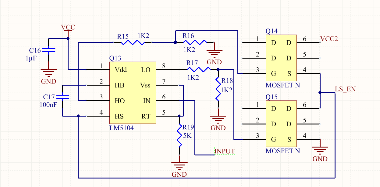
As said earlier, VCC2 can go grom 1.25 to 7Volts, and the VCC supply is 15VDC.

The mosfets used can drive the VCC2 voltage without trouble, but have a low VGSmax. That is why there are voltage dividers on both HO and LO command outputs.

The montage works as expected, meaning that the output LS_EN can be turned on and off for all VCC2 values, but for some reason several LM5104 burned while trying this montage. Is there something in that configuration that could lead to a failure of this chip ?

Regards,

Léo

  • Hi Rodrigo,

    Welcome to e2e! thanks for asking about LM5104, Im an apps eng on this device.

    VSS looks to be connected to GND through a 5kohm resistor. Can you confirm this? With this grounding configuration its possible that the driver is seeing a voltage difference between PGND and VSS causing power train current to ride on gate driver ground. VSS should be equal voltage to the source of Q15.

    Please let me know if this solves your problem or any more concerns exist.
    Thanks,
  • Hi Jeff,

    Thank you for your feedback !

    My apologies, it looks like I did not spend enough time on this schematic and did some mistakes.

    Here is a reviewed version that matches my montage :

    Regards,

    Léo

  • Hi Léo,

    Thanks for your update, here are my initial thoughts/questions:

    1) The rec op max for LM5104 is 14V so running at 15V may produce results outside expected datasheet functionality.

    2) the 1k voltage divider (and drop from the boot diode) we will expect to see about 7V on the gate of Q14. When VIN is 7V, the source of Q14 will be 7V and in order to fully turn on the highside FET the gate needs to be at least Vgs_th + 7V. So the gate to source voltage does not allow the FET to saturate properly with 7V VIN and the driver bootcap ends up working harder to fully charge Ciss. In order to fully turn on the FET we need to bring the gate past Vgs_th and the miller region plus a little more to effectively reduce Rdson.

    3) what is the duty cycle and frequency of Q14? with higher on times we will run into the issue of discharging the bootstrap too much which will create more dissipation when replenishing. The 1k divider will discharge the boot charge even faster.

    4) having a 1kohm gate resistor will slow down the rise time by 1000 times this will help with EMI and and taking away dissipation from the driver but can also lead to longer delay times and possible shoot through.

    Thanks,
  • Hi Jeff,

    Thank you for your detailed feedback.

    Jeffrey Mueller said:

    1) The rec op max for LM5104 is 14V so running at 15V may produce results outside expected datasheet functionality. 


    I am indeed out of the recommended operating conditions for Vcc. The choice to go over this rec op was made to ensure that HB would always be VHS + 8V at least. I tried with lower Vcc values, and the driver would not manage to keep VHS high if this condition on HB was not satisfied. Besides, VCC is still at a reasonable value compared to the maximum rating, do you think this could cause damage to the chip despite this ?


    Jeffrey Mueller said:

    3) what is the duty cycle and frequency of Q14? with higher on times we will run into the issue of discharging the bootstrap too much which will create more dissipation when replenishing. The 1k divider will discharge the boot charge even faster.


    The input command is not periodical and is mostly at high level, so the duty cycle is 100%. Could the bootstrap's fast discharge harm the driver ?


    I thought about getting FETs with a higher VGSmax and removing the voltage dividers from the montage in order to reduce delays and to ensure that VGS is higher than VGS_th+ VCC in every cases. But I understand from your 4th point that those resistors might releave the driver, is that right ?


    Regards,

    Léo

  • Hi Léo,

    Thanks for your update!
    Since you are running at 100%dc we will need a separate floating supply to keep the bootstrap charged up. This can be done with an isolated bias transformer like in figure 6 from www.ti.com/.../slua669a.pdf you can also check out an EVM that already has this www.ti.com/.../UCC5390SCDEVM-010

    If HB-HS dips below the UVLO falling threshold (6.2V typ) HO will stop switching. VDD=15V should not damage anything however Its possible that a negative transient on HS from high dv/dt switching is exceeding the HB-HS abs max rating for a short time. Probe HS-GND to make sure the edges have no negative transients.

    The boostrap doesnt seem to be charging so I assume this heat is coming from boostrap discharge which can be excessive since the peak current capability of the highside comes from the boot cap. But the worse case would be during start up when the boot diode has current flowing through it then HO turns on needing to quickly reverse bias the diode. Since this is in steady state and I assume the FETs are also not burned then the power dissipation is probably coming from the peak current^2*R_OH for an extended duration as well as average leakage current from the 1k. Probe HB-GND to see how the bootcap is being discharged, use same V/div as HS-GND.

    After the Cgs becomes charged at 7V wrt to HS its open circuit and Q_HB leaks out at a rate of 7/1k = 7mA and for a 100nF bootcap it will take only about 126us for HB UVLO to be reached. Probe HO-HS to see if the highside FET is staying above the Vgs_th. If not, then we may have to get rid of the divider.

    Thanks,