This thread has been locked.

If you have a related question, please click the "Ask a related question" button in the top right corner. The newly created question will be automatically linked to this question.

TPS61194-Q1: LED could not work normally,and fault showed the sch of LED is open

Part Number: TPS61194-Q1

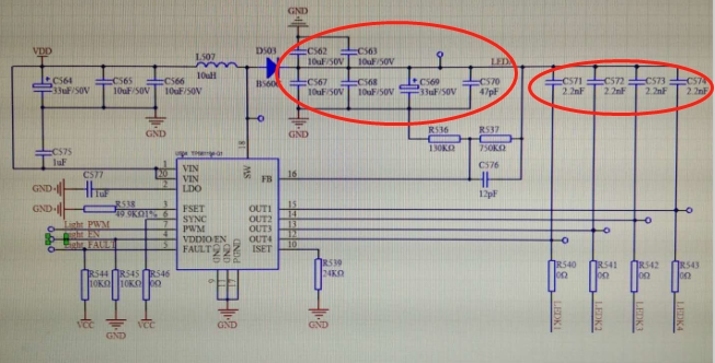
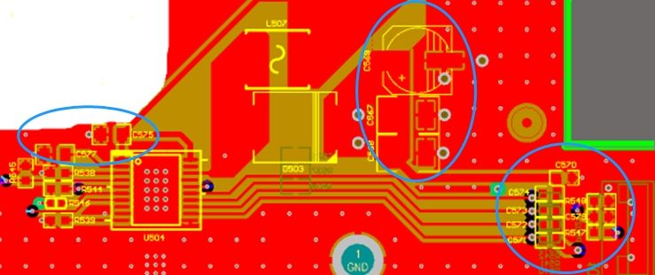
here is the SCH with layout:

We tested the waveform of OK and Wrong:

OK:

Wrong:

and test PWM to show the turn on timeline

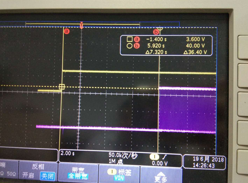
Found it may be cause by peak of SW,and continue enlarge the wavefrom of SW:

Then test the OUT1~4 of TPS61194-Q1

according to the datasheet:

Customer wonder if it is really cause by peak of VOUT,Then how to develop the SCH?There are some different Cap for this part,but still could not work well?

Or there is another reason?Customer want to apply for FA ,inorder to check the wrong in IC

Or wether it is decided by TPS61194-Q1 ? 

  • Hello,

    The team has received your request and we'll provide feedback shortly.

    Thank you.
  • Hello,

    Is this issue seen only on one device or multiple devices (with same schematic/layout)?
    Any difference between devices that work OK and NOT OK? Do they use same schematic/layout?

    From the schematic, it seems that capacitors C571-4 are connect from Boost to OUT pins which is correct, but LEDs should not be connected after capacitors in series. LEDs should be connected in parallel to these capacitors from BOOST to OUT pins. I think this could be causing LED open fault to trigger. Please let me know if this is the case.
  • hello,

    The schematic is not complete, the capacitors are paralleled to LEDs not serial. so the schematic is right. more information i will check with customer engineers.

    just now the key point, we find Vout have big peak voltage, the max voltage is up to 65v.

    1.Need your help to review the schematic and parameter, provide suggestion to clear the peak of Vout;

    2. How about the risk of max peak voltage is up to 65v, just now the OUT pin have been damaged. 

  • Hello,

    We reviewed the schematic and here are our comments below. There does not seem to be any major issues that could be causing the issue. If this is only seen in one device, we would recommend submitting for FA.

    1. FSET = 49.9k - Set for 1.2 MHz OK

    2. ISET = 24k - Set for 100mA OK

    2. Connect SYNC pin to VDDIO/EN pin instead of VCC rail

    3. FB network set to max 37.1V. Make sure max Vf is ~15-20% lower than this. Also, consider using T-divider network in order to reduce the feedback resistor values and keep Vout min higher than Vin max. Please see attached calculator to select proper resistor values. Use R2 = 6K and R3 = 27k will modifying R1 to yield proper max output voltage.

    0020.TPS61193-4 FB Divider Options.xlsx

    4. Recommended output capacitance for 1.2MHz full load condition is 3 x 10uF (cer). Can reduce output capacitance but ensure that phase/gain margin show good stability