This thread has been locked.

If you have a related question, please click the "Ask a related question" button in the top right corner. The newly created question will be automatically linked to this question.

UCC28950: DB and DC near Ls overheating problem on 600W DC-DC 300V output 400V input

Part Number: UCC28950

Good Morning

I'm trying to design a power supply controlled by the UCC28950; the input is 400V from a PFC and the output is 300V / 2A (600W), insulated from the mains.

For the design of the components i used the SLUC222C Excel file, available in the product page.

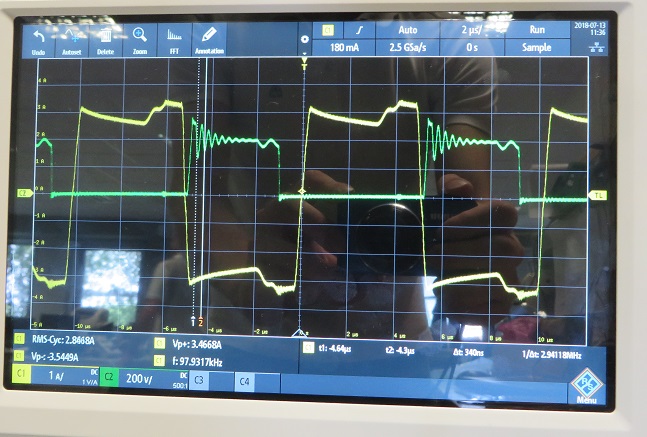
The circuit reaches the nominal power, unfortunately just for a little time with lower efficiency than expected (about 85% instead of 90%), getting DB and DC overheated. This happens even at light loads (at 100mA outpout they reach 100°C in a few seconds)

In the Detailed Design Procedure the worst case power dissipated is (Ls energy * T) -> (1/2L*i^2*f) and it says "normally they do not dissipate much power"

Does anyone have the idea of which is the possible cause of overheating of the components DB and DC, used to fix Ls potential? Which is the abnormal condition?

The circuit is without SR (unconvenient for high voltage and low level of the output current), there is a full bridge rectifier whith a passive snubber on the secondary side.

I attach the schematics, in this case diodes involved are referenced as D2 and D10 that corrisponde to DB and DC.

The part actually mounted is STTH310S, comparable to the MURS360 in the original design.

Thanks in advance and kind regards

  • Hello Francesco

    That's an interesting question -
    First thing is that the efficiency of 85% at full load implies you are losing 105Watts somewhere. I doubt if it is all disappearing into the diodes - bu that's a matter for later investigation.

    I had a look at the specs for the MURS360 and STTH310 devices and there are enough differences between them to make it worthwhile sourcing some MURS310 diodes and replacing the parts you are using - initially just for comparison. For example the reverse recovery time is longer - 75ns versus 50ns. The forward recovery time is also much longer 300ns versus 25ns. During this time the diode will have a higher than normal voltage across it and increased dissipation as a result. The Vf is also higher - partly a consequence of the fact that the STTH310 has a reverse voltage rating of 1000V versus 600V for the MURS310. The thermal resistance, junction to lead is also higher on the STTH310 device (20°KW^-1 vs 11°KW^-1).

    I would also suggest that you remove one of the two secondary windings - and compare the one winding efficiency with the two winding efficiency at half power. One would hope that the two secondaries would share current equally but that may not be the case - especially if one is wound in a different part of the bobbin than the other. If you do this, the windings see slightly different H fields and this can cause significant losses due to current circulating from one winding into the other.

    While you are doing this - it may also be worthwhile to see if there is a correlation between dissipation in the diodes and having one or two secondary windings.

    Can you double check the turns ratio you are using - I'd advise a hand calculation using Vout = D Vin (Ns/Np) the reason for this is that the Excel file calculator rounds the turns ratio to the nearest integer. This is just about acceptable where Vin is 400 and Vout is 12V for a turns ratio around 20 or so. But the rounding can give large errors where the ratio is lower - as it will be for 400Vin and 300Vout

    While debugging these UCC28950 circuits I sometimes find it useful to power the UCC28950 from an external source and then run the power train off a much lower than normal voltage - the controller will run at Dmax of course but you can observe the switching waveforms at a lower input voltage (I use something between 10V and 100V - it just depends)

    Anyhow - definitely the first thing to try is to change the diodes.

    Please let me know how you get on

    Regards
    Colin
  • Many thanks for your analysis Colin.

    I tried to lower the voltage, for example changing the feedback resistor:
    at 50Vout with 90Vin, the converter can generate 2A without the overheating of Da and Db (they reach approximately 70-80°C anyway, not negligible).

    For the reverse recovery time they are the same: in the STTH310 is indicated only the maximum of 75ns, while in MURS360 50ns is the typical time; the maximum is also 75ns.

    Regarding the forward recovery time i can't understand if they're comparable: altough MURS360 seems better with 25ns, it's measured with only 1.0A at 100A/us, to reach 1V; for STTH it's indicated 300ns but the current is triple (3A), the di/dt is half (50A/us) and the voltage is the twelve times(12V)... Anyway a parts replacement is a good idea for this check.

    The nominal ratio is 1:1; I tested with a sinusoidal voltage generator injecting 5VRMS @100khz, measuring primary and secondary voltage with a HP3457A  (capable of TRMS measure even at this frequency) after an adequate warm up: PRI=4,9454v; SEC1=4,9255V; SEC2=4,9256V.

    I will return to this task the next week and I will update you about the substitudion of the two diodes and with only one of the two secondaries running;
    any other idea is kindly appreciated.

    Regards

  • Hello Francesco

    Definitely try the MURS360 diodes.
    I would also suggest you look closely at the switching waveforms around the main transformer. They should be stable and have little if any spiking. You should also look for ZVS (check the gate drive waveform for the absence of Miller region). I would also re-check the delay times you have set.
    If you post some waveforms here I can have a look and maybe spot something.

    Regards
    Colin
  • I spend months trying to solve the same problem. The diode is not your problem. The circulating currents is!
    I ended up using sic diodes and had many issues with getting Ls right.It was extreme critical to getting the construction right.
    The problem is the low transformer premier to secondair turn ratio. So the input window for good correct resonant switching is very small.
    I think it is possible to get it right but there are extreme tolerances . Vin and Vout are one of them,
    I ended up using a hard switch full bridge and that worked straight away with a much better efficiency.

    I asked TI many detailed questions about PSFB and got little answers. So don't expect to much.
  • Hello Francesco

    Please keep me informed of your progress - In addition to the Diodes it would be worthwhile to double check that you are getting ZVS (the easiest way to do this is to look at the Vgs of the MOSFET and see that there is no Miller Plateau.

    Regards
    Colin
  • Hello Colin,

    changing the two diodes with MURS360 immediately improved the situation, giving me chanche to work on the circuit. I've also added homemade heatsink, doing so the temperature of Da and Db reaches 70°C: I think I can evaluate a standard SMD heatsink for the next prototype or to use a similar diode in TO-220 package.

    Then i could evaluate the output bridge, finding that it was causing many losses: I put other diodes and now the overall efficiency seems adequate.

    I attach the photos of the home made heatsink and the new efficiency table.

    In reply to evs: thanks for the advice. I've done some simulations and SiC in this case would not change much for me, I think for the high frequency ringing which would pass throug the junction capacitance, producing heat.

    I take the opportunity to ask: I scoped this primary waveform in jellow, which is not like the literature (the green one is the voltage across one rectifier) :

    do you have any idea about this? Maybe is it due the output snubber which stores energy?

    To conclude, after this promising results unfortunately the specification have changed and now i have a 360Vinput, forcing me to do all the calculations and the construction of a new transformer which elevates the secondary voltage.
    The calculations are made in the same way of this working prototype and the PCB is the same, but i am facing with several instability of the controller: it seems that it changes very fast in duty cycle with ondulation in the peak current, also audible noise (and the disconnection of a near USB mouse too...).
    I tried to evaluate the EA input at low voltage al 100% of duty cycle, but this causes  instability so i am worried. I will work on it and would like to have help on it reporting the problems noticed: do you think I need to open another thread or continue in this?

    Thanks and Regards

    Francesco

  • Hello Francesco
    It's great to hear that you have made some progress. Specifications get changed from time to time of course but at least you don't have to go all the way back to the starting point.

    I'd make a few comments - first, it is clear that the diode is getting avalanched at the start of the turn off interval. This should be avoided - ideally one would reduce the amount of unclamped inductance in the diode path (short wide PCB traces) and also improve the snubber design so that the ringing is damped out more quickly than is shown here. Initially at least I would work with output diodes with a higher breakdown voltage. it also seems here that the output inductor current is discontinuous - is this what you expected at the operating conditions when the picture was taken? I think that you are correct that the current waveshape is due to the output snubbering - but I have to double check this with some colleagues.

    Can you send me your PCB layout and I can have a look to see if there is something obvious that may be causing the instability - please send it to me at colingillmor@ti.com (Gerber files or native layout files are best for me.)

    Let's leave this thread open for now - it keeps everything in one place.

    Regards
    Colin
  • Mr Colin,

    I imagine that the main cause  of the overshoot  is the secondary leakage inductance: is that correct?

    I think inductor is conducting correctly, please confirm regarding the waveforms that i took at 600W out...

    Shown here:

    green = secondary voltage (differential probe 25Mhz), yellow = inductor current (1:1 probe 5Mhz)

    here:

    Green = inductor voltage, yellow inductor current, orange primary current with a 200mV/A ->This probe is only 500kHz of BW, so please consider it just as a reference (the real shape is shown in the previous reply)

    Please consider also that the frequency in the inductor is 200khz, the oscilloscope its evaluating it  wrongly probably for the spikes.

    To support the overshoot is currently mounted a 1200V ultrafast rectifier at the secondary side.

    I'm sending you gerber files via email.

    I'm not a power supply specialist, so I am learning a lot from you: i would like to thank you for the support.