This thread has been locked.

If you have a related question, please click the "Ask a related question" button in the top right corner. The newly created question will be automatically linked to this question.

LM5176: LM5176: BOOT1, HDRV1 with respect to SW1 issue

Part Number: LM5176

Hi:

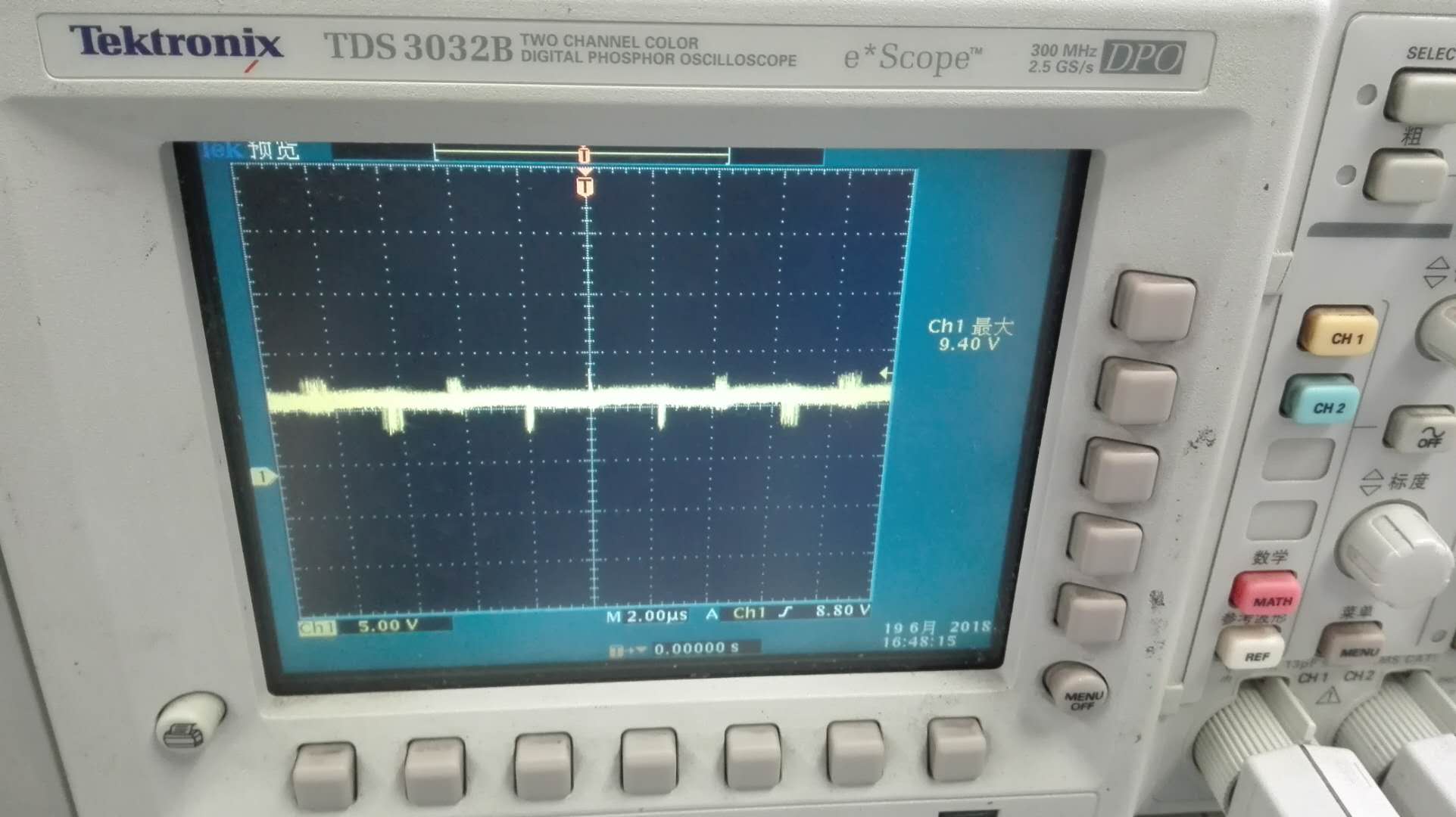
In the LM5176 datasheet, BOOT1, HDRV1 with respect to SW1, the range is -0.3~8.5V. 

We test the voltage is 9.4V(max). Does this means the BOOT pin will damage? How to adjust this? 

Another issue, when switch the converter off and then on(in 10 seconds), the Boot and HDRV pin will damage, (100%). Is this part cannot switch off/on fast?

8546.SAWA-81-45020A -SCH.PDF

  • Sorry I could not understand what this 9.4V is referring to on your scope picture. It does not look like V(HB)-V(SW) or V(HO)-V(SW). It is more look like HO or HB voltage to GND.

    Did you say you switched off and on i n 10sec, or 10 us? They are big different. And, how do you do to switch the converter on and off?
  • Hi:
    The 9.4V on the scope is the voltage between BOOT1 and SW. the range on the datasheet is 8.5V, how to adjust it?
    Switch the converter off and on is in 10 sec, not 10 uS, the customer need test this point, is it means this part cannot switch off/on fast?
    Thanks for your reply!
  • Hi Henry,

    How are you turning the device on and off? It it just by lowing the input voltage? Does the output voltage decay all the way down to 0V?

    The voltage from BOOT to SW is set by the VCC regulator. The VCC regulator output voltage is not adjustable. Please note that D4 and D5 should be schottky diodes.

    Thanks,
    Garrett