Because of the holidays, TI E2E™ design support forum responses will be delayed from Dec. 25 through Jan. 2. Thank you for your patience.

This thread has been locked.

If you have a related question, please click the "Ask a related question" button in the top right corner. The newly created question will be automatically linked to this question.

LM5175: VCC pin change from 7.36 to 3.4V and IC is not working

Part Number: LM5175

Hello,

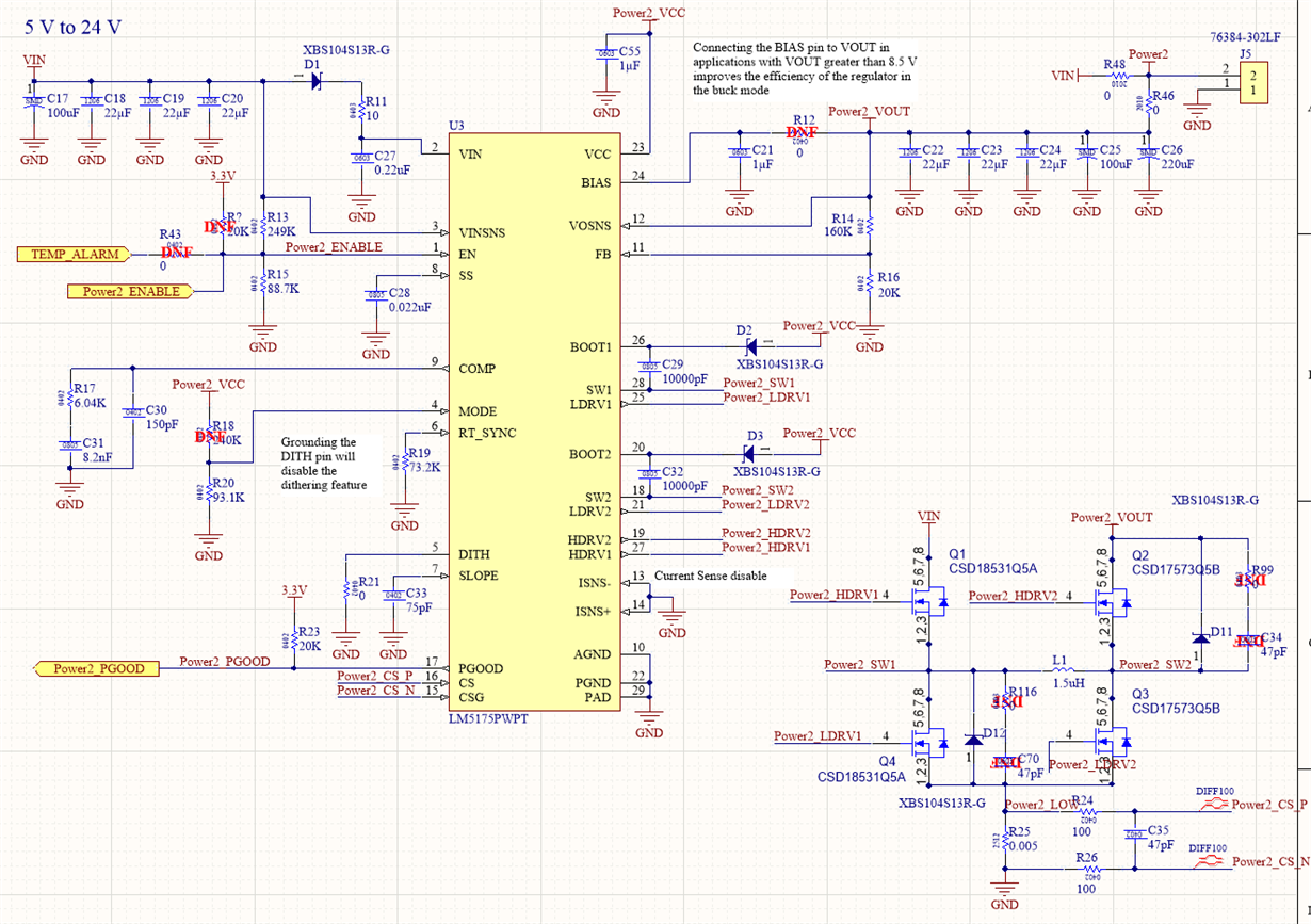
We designed a buck/boost DC-DC based on the LM5175. The input is 5V to 24V with an output of 7.2V and 10A.

Sometimes after a unexpected load, the VCC pin get 3.4V and the IC stop working once a small load is applied (~0.2A).

Some values during normal operation:

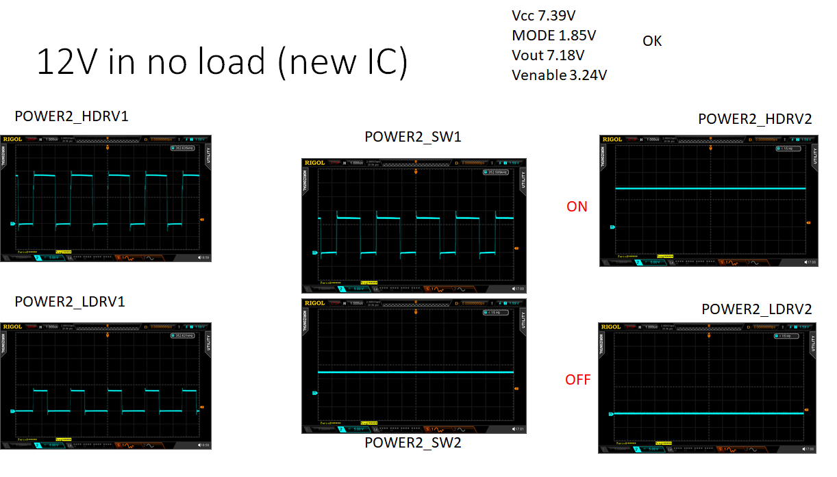
  • Vcc 7.32V
  • MODE 1.85V
  • Vout 7.18V
  • Venable 3.23V

Once the IC stop working, the new values are:

  • Vcc 3.4V
  • MODE 1.85V
  • Vout 7.18V
  • Venable 3.23V

I'm not sure what is causing the unexpected load in the circuit, neither why the IC could be damaged once a high load is present (if this is the cause). 

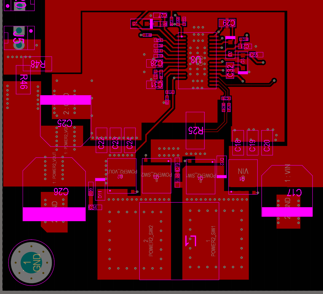
Another situation we found during testing, was an audible sound when the power input is decreased (voltage and current). We follow suggestion about finding the source with a pencil, but was very hard to located. The level sound increase when the input power is reduced (voltage or current).

Any advice pointing to a solution is appreciated.

We are going to manufacture a second revision and would like to include any improvement to avoid these situations. 

Thanks

Hu Lao

  • Just to clarify, the output is 7.2V without load. Once a load is applied, the voltage decearse to almost zero. All the external components seems to be working, because once the LM 5175 is replaced, everything start working.
  • Dear ,
    I checked all the LM5175 post and you are involved in many of them, offering solutions to customer issues. I didn't find a similar situation as mine. I appreciated if you could take a look to the situation reported in this post.
    Thanks,
    Hu
  • Hi Lao,

    What do mean by and unexpected load?
    Can you only achieve 200mA load before the LM5175 is damaged?
    What is the input voltage condition that you see this happen at?

    On quick suggestion to test is populating the snubber (R99 C34) that is on the boost leg.

    -Garrett
  • Hi , thanks for your feedback.

    I answer to your question in the same order:

    • Unexpected load: the DC-DC is powering a thermal printer. Sometimes, the print job contains high density black content, which cause high current in the DC-DC output.
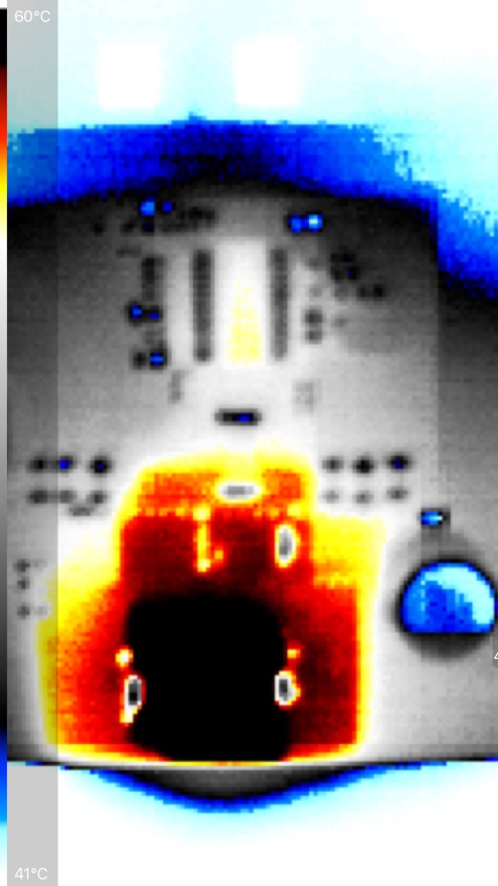
    • Before the LM5175 is damaged. With an power bench supply, we set the input from 5 to 24V [3A max]. We place a load simulator in the output, getting all the power from the input. We change the input voltage from 5V to 24V while the load is active. NOTE: we need to adjust the load to don't pass the input power. When that happens, the circuit emit sounds. This is something that we are troubleshooting (following suggestions from other posts).
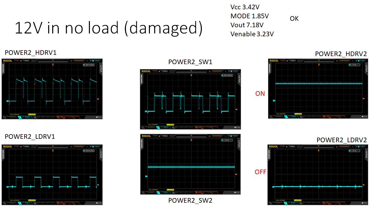
    • When the LM5175 get damaged, the input voltage is fixed to 12V [with 3A max]. We figure out the IC get damaged, because the current increase in the input. Not sure yet if the cause is because the current is high during too long or because a high voltage in the somewhere. Trying to solve this issue, we monitor the PGOOD and disable the IC once the pin get to zero. In this case, the IC get damage as well. 

    We already damaged many IC. We also try figure out a condition using the load simulator, but not lucky to find yet.

    Thanks for the suggestion. We are going to try that. Please, may I know your consideration behind the suggestions? Is to avoid high voltage in SW2 that put the diode D3 in reverse and causes problem in the VCC pin? In that case, do you think that a zener diode in boot capacitor C32, could also help in this regard? We just trying to understand the cause/reason the VCC regulator get damaged. 

    Thanks again,

    Lao

  • Hi Garrett Roecker (3456925) ,

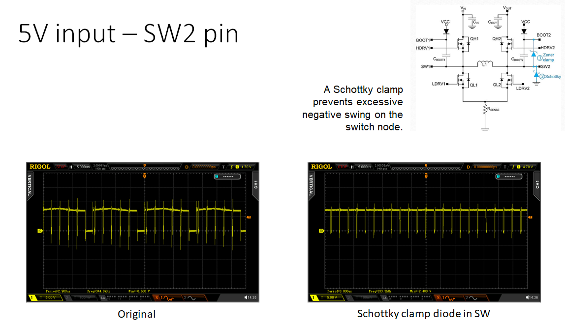
    We update the PCBA including a schottky clamp to prevent excessive negative swing on the switch node. Refer to attached figure for results.

    We perform new testing on the board including new equipment, and we was able to use a input of 5V to 24V [with max 20A] and simulate a load up to 10A. The results was OK in all the range.

    At the end, we was able to damaged 2 of 2 IC, with a "short circuit" test. So, right now, we have a defined test condition to damaged the IC, with the symptoms mentioned previously. Knowing  this condition, may you why the IC short circuit protection is not working as expected?

    Thanks

  • Hi Lao,

    Can you please take some screen shots of when the device is being damaged? It would be good to monitor the buck and boost switch nodes as well as the VCC voltage. Maybe when the output is being shorted there is an over voltage on one of the pins that might be causing the damage.

    Thanks,

    Garrett