This thread has been locked.

If you have a related question, please click the "Ask a related question" button in the top right corner. The newly created question will be automatically linked to this question.

LM5050-1: LM5050-1 function question

Part Number: LM5050-1
Other Parts Discussed in Thread: LM5060

1. Wide Operating Input Voltage Range, VIN: 1 V to 75 V (VBIAS required for VIN < 5 V) : VBIAS Refers to VS Pin need???
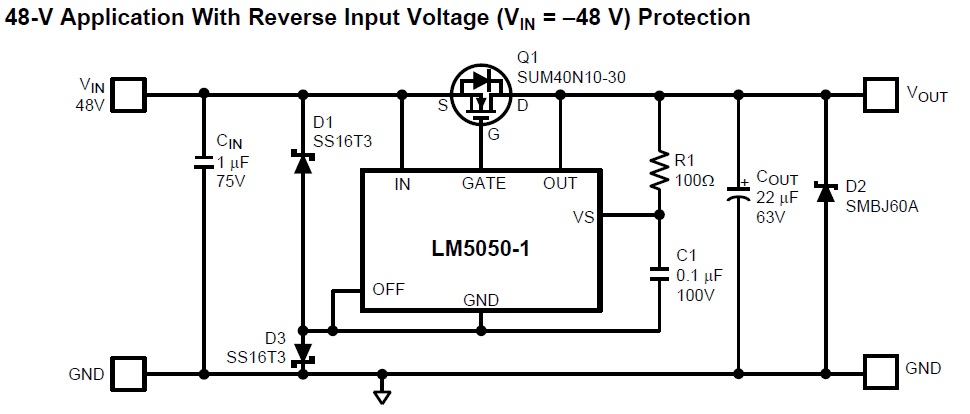
2. Fast 50-ns Response to Current Reversal : Output Reverse Current Reverse Input Protection????
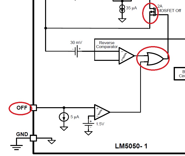
3. OFF pin passes OR-gate, how to control MOSFET ON/OFF function???(Page 12)

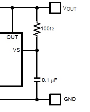
4.VS-Pin external resistor fixed with 100 ohms:  Is there a disadvantage to using a larger resistor? Or other side effect???

5. MOSFET selection :  Low Rds(ON) is generally selected. This IC-specification content does not necessarily use low RDS(ON), but it also involves hot issues.
                                    The recommendations are as follows (22 mV / ID) ≤ RDS(ON) ≤ (100 mV / ID) The content is not very clear, can explain why the low RDS(ON) mechanism is not selected?

6.
A.  Can be explained as follows in the Reverse Input voltage protection, as long as the function of the LM5050-1 is not needed, the power supply of the LM5050-1 can be disconnected by turning off the Q2, which means the turn-off IC?
B. The following circuit can explain ON/OFF Control  D2  D3  Q2  loop and function operation
C. Why IC GND-Pin does not need to be connected to earth-GND???

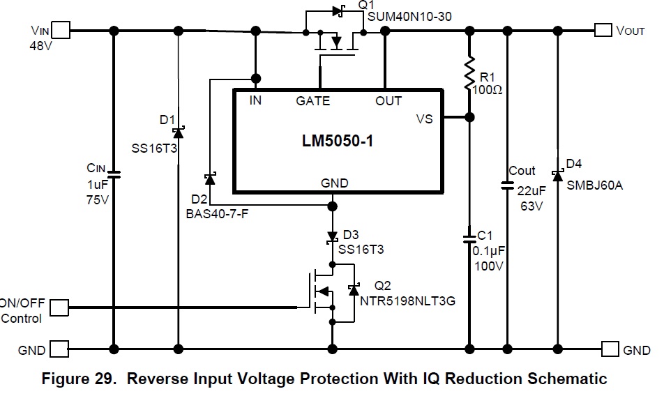
7.  Do not understand, use D3 when IC reference GND??? Can explain in detail and function

  • Hi

    1. VBIAS refers to Vs pin. Vs pin can be connected to separate supply for VIN <5V.
    2. Fast 50ns response is for the reverse comparator to trip after detecting a reverse current (output to input, can be due to reverse input polarity or ORing power supplies). When a reverse current starts to flow from out to input, reverse comparator sense it by measuring the voltage across IN-OUT. And turns off the external MOSFET by connecting Gate to IN through 2A strength internal MOSFET.
    3. Yes, when the IC is disabled, Body diode of external MOSFET passes current. To cut off the power path, need have back-back FETS. LM5050 can not drive two back to back FETs. So recommended to use LM5060 and additional MOSFET for power path cutoff.
    4. Larger resistor for VS-Pin is not a problem, but should not be very big >10k. what resistor value do you plan to use?

    Let me get back on the rest of the questions soon, today.


    Regards,
    Kari.
  • Hi

    5. MOSFET selection: Low Rds is generally selected, but however it should not be very low, which means larger size and more costly. LM5050-1 is linear regulation of Vds across the MOSFET to 22mV, that is Gate of the MOSFET is controlled so that across most load currents, 22mV is maintained. This has advantage of turnoff faster during reverse current or reverse polarity situation and enables smoothing switch over during ORing of power supplies.
    MOSFET is sized based on the regulation threshold. To be precise, RdsON = 22mV/I_Nominal, based on the nominal current which flow most of the time. Selecting a MOSFET bigger than this, means lower RdsON, which means MOSFET is near to Vth of Gate and not fully enhanced. Operating close to Vth means, there is a chance of light load oscillations. RdsON is chosen around 22mV/I_Nominal.

    6. Reverse input voltage protection with Iq reduction: When Q2 is turned OFF, LM5050-1 IC is not powered, no GND connection. So IC will be OFF. Q2 is required to reduce the Iq supply current flow through the IC. When Q2 is OFF, it breaks IC GND from earth-GND (system GND). This circuit is enabled using ON/OFF control. When the control is OFF, the whole circuit is placed in low Iq state and LM5050-1 is disabled(unpowered) due to lack of GND connection.

    7. Use of D3: D3 is required for reverse input or reverse polarity protection. Lets say a reverse Vin is applied, now if D3 is not there, there is a path for the current through GND-->ESD diode from GND to IN-->IN, this literally short the input to GND and huge current can flow from GND-IN. D3 blocks this reverse input and protects the IC and downstream circuit.


    Regards,
    Kari.