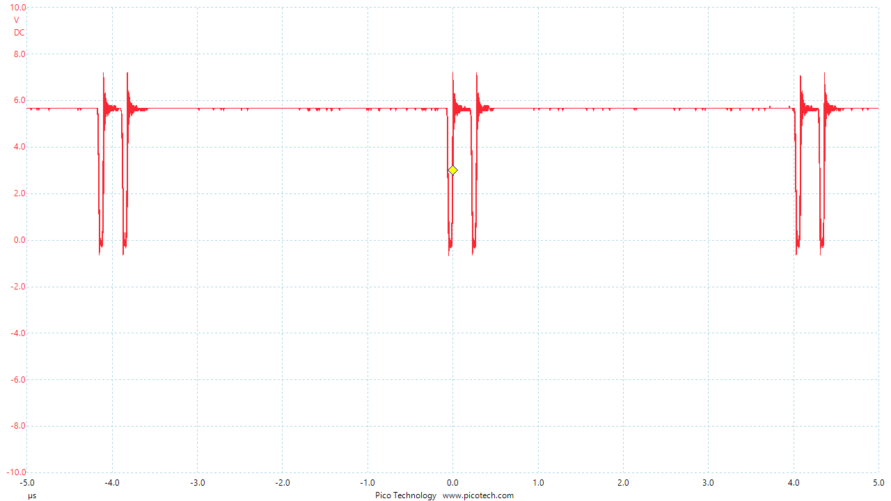
Please note this waveform:
The signal shown above is the input to the inductor from the PMOS FET. The TOFF setting is 4. The probe is 10X and I forgot to set it as 10X so the scale on the left is /10.
Other relevant settings: L = 390 uH. Rsense = 0.2 Ohm 1%. The dual 1uF output caps have been removed from the evaluation board. IMAX is set to 255. The diode load is roughly 53.6 Volts and Vin is 57.5 Volts. (The input and load voltages are non-negotiable hard specifications that I have to meet, all other parameters and values are fair game.)
The transistor is nearly in saturation and half the time it takes quite a while for the output current to get to IMAX. The other half of the time IMAX is reached very quickly.
That behavior seems abhorrent to me.
Questions:
1. Is this behavior expected? If not, is there a way to fix it?
2. The average frequency is still within the tolerance of the part, but the frequency of the back to back pulses is way too high. Even if it is abhorrent, is this behavior okay from a design perspective? In other words, am I damaging the part running it like this?
This will cause the ripple to go higher than desired (I'm trying to keep the ripple down to 50 mA), I'd really like to be able to get the frequency to around 800 KHz. With this double pulsing, the ripple will be almost double, even if I get the average frequency to 800 KHz.


