This thread has been locked.

If you have a related question, please click the "Ask a related question" button in the top right corner. The newly created question will be automatically linked to this question.

TPS92692-Q1 Question

Part Number: TPS92692-Q1
Other Parts Discussed in Thread: TPS92692

Hello TI,

1. Does 692 can operated above 65V LED voltage by B2G topology? consider have enough stress on switch componntor.
2. Look 692 DS show max duty cycle 93%@ 390kHz. What is the maximum out voltage capability?
3. Does RCS can place low side(GND)? consider good route.
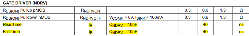
4. 692 output spurce / sink capability of DRV pin? below is MAX20090 spec.
5. Could you commend for TPS92692 better than MAX20090?

  • Hello John,

    I assume B2G is boost to ground, or is it something else?

    If it is a boost:
    1) Yes but the current sense will have to move to the bottom of the LED stack.
    2) Maximum output voltage is dependent on minimum Vin, typical maximum duty cycle is 90% per the datasheet.
    3) Yes.
    4) Gate pulling high is 5.4 ohm typical, gate pulling low is 4.3 ohm typical.

    Regards,
  • Dear Sir,

     1) Yes but the current sense will have to move to the bottom of the LED stack.
     Move to buttom of LED stack because high side induce higher power loss on resistor(V*I), right?

     4) Gate pulling high is 5.4 ohm typical, gate pulling low is 4.3 ohm typical.
     So, MX20090 looks source/sink capability strong than TPS92692. Could you help us to provide math about pulling high/low ohm transfer to Ampere?

    Thanks!
    John

  • Hello John,

    1) No, it's because if you decide to run above 65V the CSP and CSN pins are not rated for that. Power loss in the resistor is I^2*R or V*I. The current in the LED string is the same at the top and bottom, the resistor will also be the same value to get regulation so the power dissipation is the same regardless if it is at the top or bottom.

    4) This depends on the MOSFET you are using and how much current you are trying to regulate. Basically for turn on the current during the switching transition is (Vgate high - Vgatethreshold)/Ron and the turn off current would be Vgatethreshold/Roff.

    Example, Vgatethreshold at 4V, Iongate would be (7.5V-4V)/5.4 ohm = 650 mA, Ioffgate would be 4V/4.3 ohm = 930 mA.

    Regards,