Other Parts Discussed in Thread: BQ76920, BQ78350, , TIDA-00792
I design my bq76920 board according to the document slvu924c :bq76920 Evaluation Module User's Guide
yet, I find a strange phenomenon
I disabled the DSG MOS and the CHG MOS using FET_EN command in bqStudio.
And the DSG MOS and the CHG MOS are closed definitely, their Vgs are both 0V.
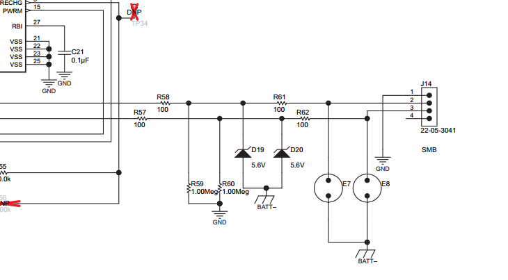
I connect three wires GND, SMBC, SMBD to my power board GNG, IIC_CLK, IIC_DATA,
And I connect PACK+ and PACK- to my power board to supply power for it.
I apply a 0.5A load to my power board.
The read current of bq78350 is 0A. but my power still can supply the desired current.
I guess the current runs through the GND of SMBus.
Because PACK+ and BATT+ are connected directly, and my power board connects the negative electrode of the battery through the GND of SMBus.
As a result, the battery is connecting with my power board directly regardless of the status of the DSG MOS and the CHG MOS .
I think this is a serious mistake.
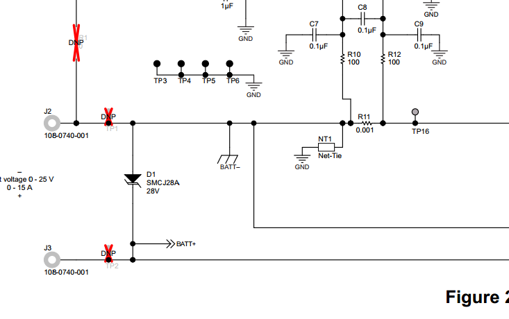
In another design document, named tidrqy7 of TI, the DSG MOS and the CHG MOS connect to positive electrode of the battery.
And I think this design doesn't have such a problem.
What is the component NT1 connecting the BATT- and GND?
I didn't use such a component, I use the BATT- to be the GND.
Am I right? Should I use the Schematics of document tidrqy7 instead of document slvu924c? How can I solve the problem?