This thread has been locked.

If you have a related question, please click the "Ask a related question" button in the top right corner. The newly created question will be automatically linked to this question.

LM5035: How the circuit of the optocoupler part of the LM5035's evaluation board circuit is mathematically modeled to build the power switch transfer function

Part Number: LM5035

Hello, I am studying your LM5035 half-bridge circuit evaluation board. I want to mathematically model the half-bridge circuit on the evaluation board to write the open-loop transfer function of the power supply.

However, I can't write the model of the LM5035 optocoupler part. Because the output side of the optocoupler's transistor is a current signal entering the COMP pin of the LM5035, it is different from the conventional voltage signal entering the COMP pin of the control chip.

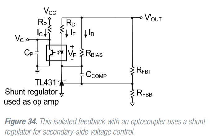
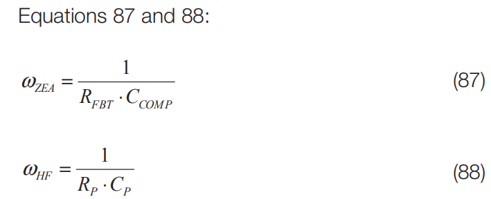
Refer to the 34th picture and the formulas  88 in the application report of "Switch-mode power converter compensation made easy" written by your experts Robert Sheehan and Louis Diana, as shown below:

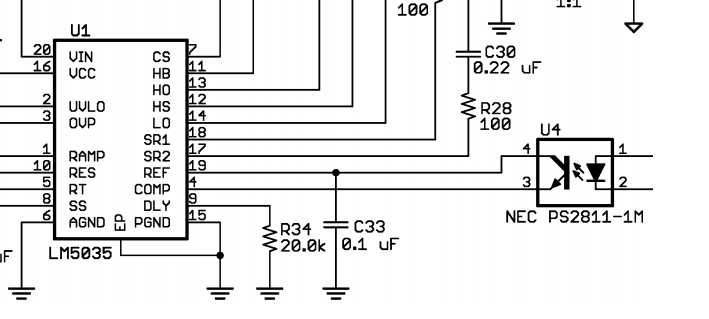
Usually, the controller will input the voltage signal into the COMP terminal, and the resistor Rp will be connected in series on the transistor side of the optocoupler, so that the pole of the optocoupler can be calculated according to the formula 88. The LM5035 is the current signal into the COMP terminal, the circuit diagram is as follows:

As shown above, I can see that the Cp capacitor is C33, but I don't know what the Rp resistor is.

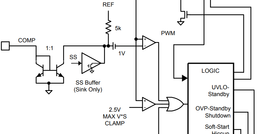
I saw the internal circuit diagram of the LM5035 chip, as follows:

Is that Rp a 5k resistor inside the LM5035?

I don't really believe that Rp will be the 5k resistor, because if Rp is a 5k resistor, the pole of the optocoupler is fz=1/(2*pi*C33*Rp)=1/(2*pi*0.1uF *5k)=318Hz, the frequency of this pole is too low, and the optocoupler pole is usually at 10kHz, so I am confused, what is the Rp value, how to measure or calculate?

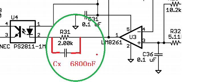
I have another problem. When debugging, I connected a 6800pF capacitor Cx in parallel with the resistor R31 on the optocoupler diode side. This capacitor Cx is good for loop stability. But I don't know how to build this Cx equivalent model.

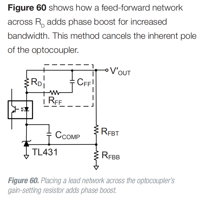
The 60th picture of Robert Sheehan and Louis Diana's application note describes a similar circuit that says it can offset the poles produced by the optocoupler, as shown below:

I think the Cx I added should have a zero effect, which improves the phase margin, so the system stability will be better.

However, I will not mathematically model Cx. I don't know how to calculate the frequency position of the zero point brought by Cx.
I look forward to your help, thank you!

  • Hi Zoujiangyilang,

    As you correctly observe the parasitic capacitance across the opto-transistor limits its bandwidth when it needs to generate a voltage signal. Typically this bandwidth limitation must be modeled since it may impact the control response and stability of the overall loop.

    Using an internal current mirror to read the opto transistor current greatly improves its bandwidth because the voltage across the opto-transistor changes very little. The internal transistor used to convert the mirrored current into a voltage has much lower parasitic capacitance than the opto-transistor.

    I cannot understand your problem in modeling Cx. The parallel combination of resistor and capacitor will look like a 2K resistor at low frequency. This will change at the frequency where the impedance of the capacitor is equal to 2K. Above this frequency the overall impedance of the network will fall with frequency. In your application this will provide flat gain at low frequency, and then increasing gain with frequency, since the opto current will increase with applied voltage as frequency rises.

    I hope this addresses your questions clearly.

    Joe Leisten

  • Thank you for your guidance!
    That is to say, the pole on the side of the optocoupler transistor is not generated by the 5k resistor built inLM5035 and C33 , but by the 5k resistor built in LM5035 and the equivalent capacitor Cinner of the built-in transistor of LM5035.
    and this Cinner is much smaller than C33 =0.1uF, what is the Cinner valuation? How many nF? Or dozens of pF? So is the pole frequency fz of the optocoupler equal to 1/(2*pi*5k*Cinner)?
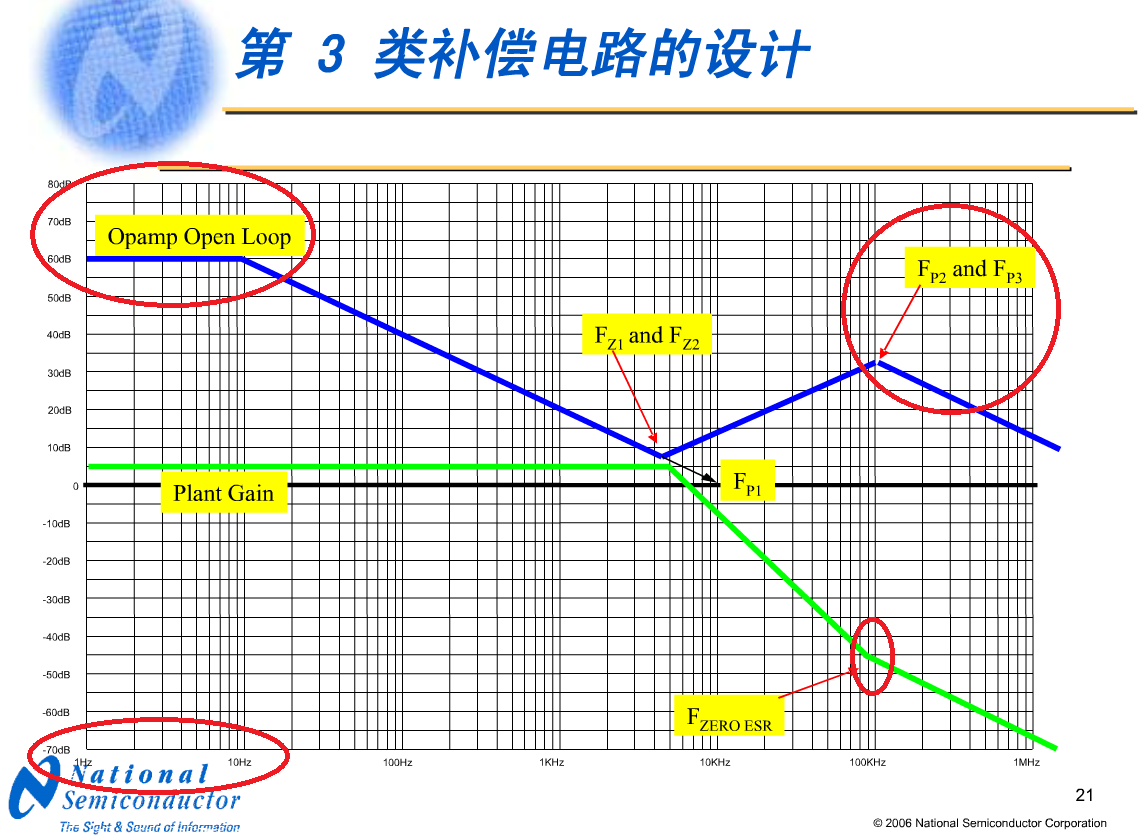
  • Hello, the picture above is the analysis of the principle of the type III compensation circuit of the LM5035 evaluation board from National Semiconductor I found online.

    I have two doubts about this bode diagram.


    1, why does the compensator's gain in the low frequency range of 1Hz~10Hz remain unchanged, instead of decreasing according to -20dB/dec?


    2. Why do the two poles Fp2 and Fp3 of the Type III compensator are placed at the zero point of the main power ESR?

    I saw in some application documents that there is a saying that Fp2 is configured at the zero point of the ESR, and Fp3 is configured at fs/2 (fs is the switching frequency) or fs or 10fc (fc is the crossing frequency). Where is this Fp3 configuration better?

  • Hi Zoujiangyilang,
    I will try to find out the value of Cinner and get back to you.
    Joe Leisten
  • Hi Zoujiangyilang,
    1) The error amplifier device has a finite open loop gain. Once you reach this level the gain is flat with frequency.
    2) The output capacitor gives us a zero, and hence for frequencies above FZERO_ESR we can remove one zero from the compensator. In theory this is all that is required but in practice it is normal to remove another zero from the compensator at some point before fs/2. Keep in mind at these high frequencies the response of the power stage may depart from the green line, and we want to ensure that loop gain cannot start to increase again at high frequencies.
  • Thank you for your advice, I understand it.