This thread has been locked.

If you have a related question, please click the "Ask a related question" button in the top right corner. The newly created question will be automatically linked to this question.

WEBENCH® Tools/LM27762: Thermal pad not connected

Part Number: LM27762

Tool/software: WEBENCH® Design Tools

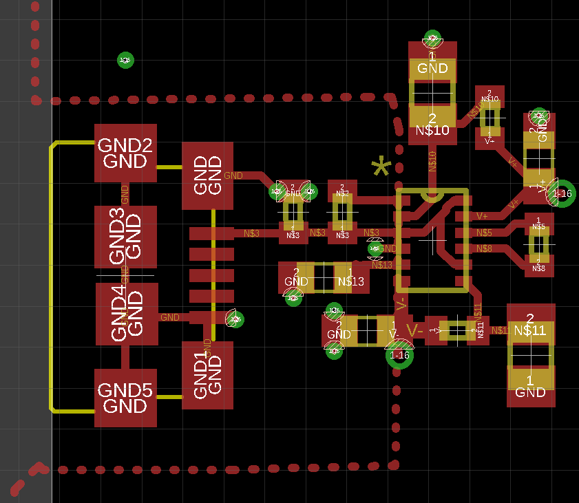
I use a LM27762 regulator to convert the +5V to +3.3V and -3.3V. I used the webbench to design the circuit. But to easy to layout the PCB board. I deleted the PAD under the chip and the thermal pad is not connected to the ground. 

Now the chip doesn't work and the +VOUT is 1.5V and the -VOUT is 1.2V. What's the problem? I see the manual of LM27762 state that the thermal pad MUST be connected to the ground. But I think it is just question about the cooling the chip and shouldn't have any influence on the voltage conversion. Am I right?

Any help will be appreciated. Thanks a lot.

  • Hi Ming,

    Yes, the thermal pad must be connected. This device uses LDOs so it will dissipate quite some heat.

    We recommend ordering the EVM to test a known working circuit in your system.
  • Here are the schematic and the pcb layout. Please help me. Thanks.

  • Thank you for replying. I know that the thermal pad is used for dissipate the heat. But I think it doesn't affect the output voltage, right? Now my problem is that the output voltages are wrong, both the positive and negative. I have posted the schematic and PCB layout here, would you please help me to solve it? Thank you very much.
  • Thanks for sharing your schematic and layout. The schematic looks ok, but none of the GND connections for the various passives connect directly back to the IC GND as they should. This can cause issues.

    The lack of a thermal pad connection can cause the IC to get very hot and enter thermal shutdown.

    If you want to debug your board, instead of testing on the EVM, you need to look at the various waveforms (Vin, CP, OUT+, OUT-, etc.) and see what is amiss.
  • Hi Chris, thank you for helping me. You mentioned that "none of the GND connections for the various passives connect directly back to the IC GND as they should. This can cause issues". I don't understand what is the meaning. I have connected the ground pin to the ground net on the PCB. This schematic is from the Webbench Designer. Is there any wire I didn't connect?
    Another question is would you please tell me what kind of waveform, such as VIN CP OUT+ OUT-, looks like? Now I have checked the pin. The Vin is a DC voltage and the amplitude is 5V. The FB+ and OUT+ are 1.50v DC around. The FB- and OUT- are 1.2V DC around. The CP is 0V DC and the voltage between the C1+ and C1- is 0V DC. I think the oscillator inside chip doesn't work. Would you please help me? Thanks a lot.
  • Hi Ming,

    The GND comment was about the PCB layout. You can see the example layout in the D/S--all the GND routings go right back to the IC's GND pins.

    It sounds like you measured DC voltages, instead of looking at each pin with the scope. The scope gives much more information.