Hi all,
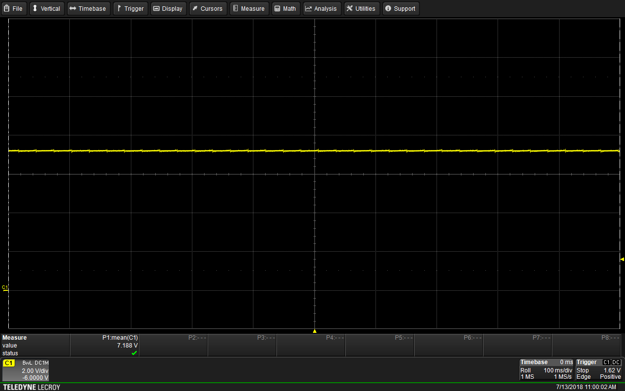
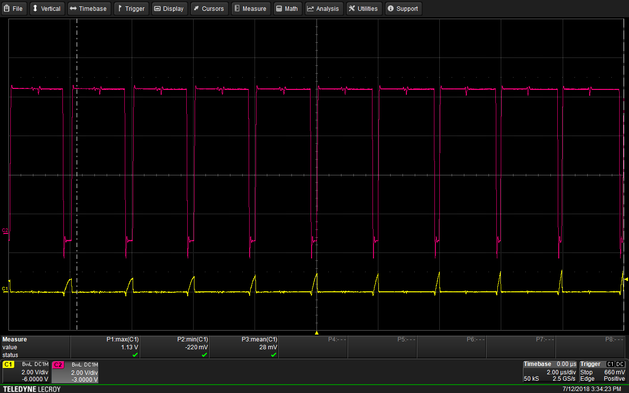
Good day, i though i met something abnormal at EN1/SS1 pin,as figures below,is there anything that we should pay special attention to? thanks.
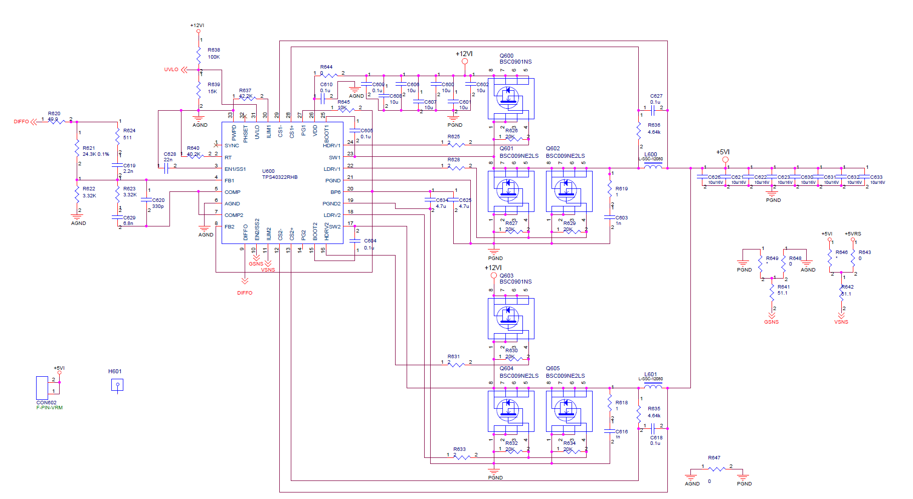
Can you help to review TPS40322 schematic and give your comments?thanks.
Vin : 12V (typical)
Vout : 5V
Iout(max) : 40A
CH1:EN1/SS1 ,no load test
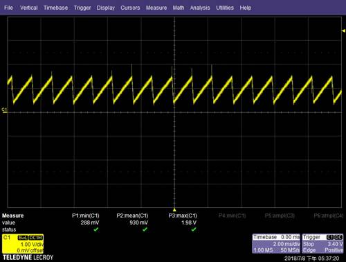
VDD & UVLO waveform
CH1:VDD , CH2:UVLO

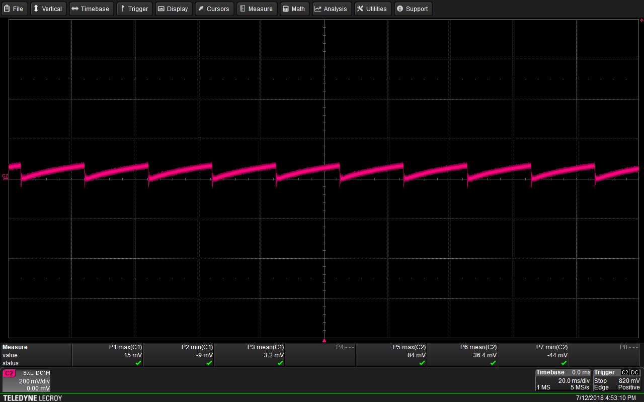
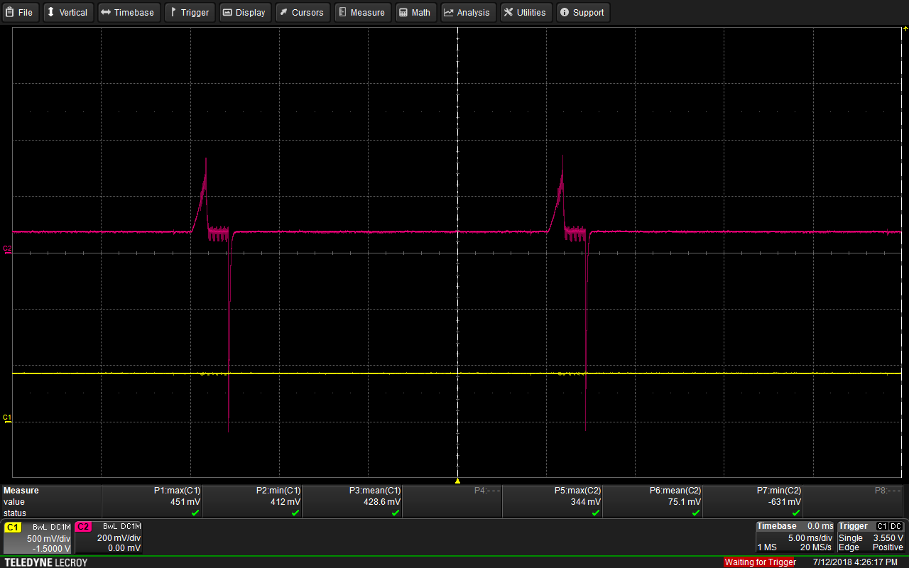
CH1:HDRV1 , CH2:LDRV1
CH1:HDRV1 , CH2:LDRV1
CH2:Vout
CH1:ILIM1 CH2:FB1
SCH file,