This thread has been locked.

If you have a related question, please click the "Ask a related question" button in the top right corner. The newly created question will be automatically linked to this question.

UCC24610: No gate signal

Part Number: UCC24610

Dear all,

We are facing the problem that there is no gate drive signal from the IC.

This is the synchronous rectification schematic for our LLC converter. 

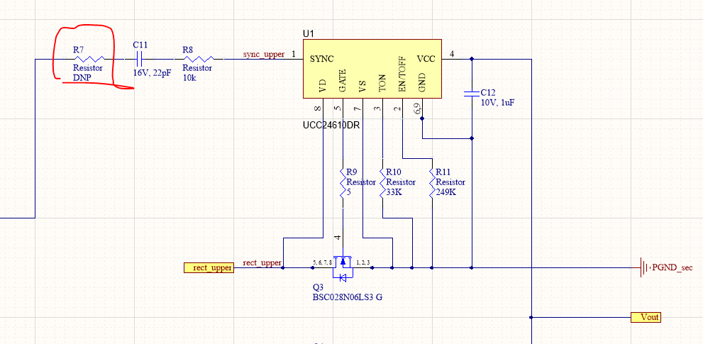
Vout is 4.9 Volts, Synch is floating, EN/TOFF is 2.5V

Here is a screenshot from the scope:
CH1 current through rect_upper
CH2 gate voltage (GATE pin 5)
CH3 voltage at rect_upper (VD pin8)

Thank you and best regards

Eyke

  • Hello Eyke,

    The gate drive should activate when the drain of your FET is 80mV to 220 mV below ground. You are more than 300 mV below ground. I wonder if there is enough VCC voltage on the UCC24610 to turn on the IC.

    The VCC UVLO turn on is specified between 4.15V and 4.65V. To ensure every device turns on this voltage needs to be more than 4.65V at turn-on before gate driver begins switching.

    I believe the device is not turning on because VCC is not high enough to meet the UVLO turn-on threshold. Could you retake these wave forms with the VCC voltage as well, just to double check this?

    Regards,

    Mike
  • Hello Mike,

    thank you very much for your quick reply.

    The requested waveforms:

    CH1 current through rect_upper
    CH2 gate voltage (GATE pin 5)
    CH3 supply voltage (VCC pin 4)
    CH4 voltage at rect_upper (VD pin8)

    The voltage is quite stable at 4.9V. Same behavior can be seen for both synchronous rectifier ICs.

    If the IC was in UVLO, as far as I understand, the Enable pin would be tied to ground. However, we measure 2.5V, which matches the 10uA and our 249kOhm resistor.

    Thank you and best regards

    Eyke

  • Hello Eyke,

    Thanks for taking the wave forms and it looks like there is plenty of VCC at 5V.  The following could be the issue.

    1. The minimum off time resistance  R11 may not be the correct value.
      1. With 249k for R11 I calculated a 1.93 us for a typical off time.  This should be O.K. for application since your off time is roughly 3 us shown by your wave forms.
      2. I reviewed the data sheet and if R11 REN/TOFF < 70K ohms the device will be in sleep mode. (Page 21, Bottom Paragraph)
        1. If R10 and R11 were swapped this would make REN/TOFF = 33 k ohms and the device would be in sleep mode and would not start.
          1. Could you double check these values to make sure they are correct.
    2. The IC could damaged.
      1. Try another IC.

    Regards,

    Mike