This thread has been locked.

If you have a related question, please click the "Ask a related question" button in the top right corner. The newly created question will be automatically linked to this question.

LM74670-Q1: LM74670-Q1 Fuction block diagram question

Part Number: LM74670-Q1

Dear team,

My customer Hikvision asked about the based function of LM74670-Q1. Could you please help? Thanks a lot.

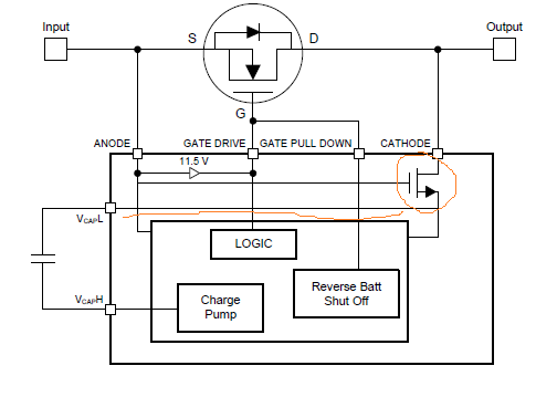
1. What is the operating principle of the CATHODE MOS? Why VcapL is connected with its Source pin?

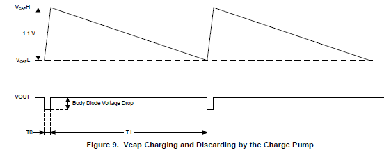
2. In 8.1.2.2, the body diode on time is 25ms, larger than the period of 50Hz, the MOSFET will not turn on. 

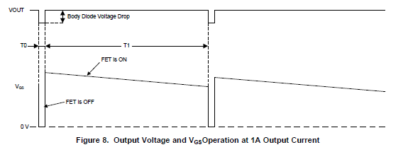
3. Why does below waveform have spike in Vgs and Vout?

  • Hi Rory,

    1. Cathode MOS is used to isolate the cathode when anode goes low (to GND or negative). This way cathode pin of LM74670 does not see high voltage with respect to its anode pin. Abs Max allowed voltage across Cathode-Anode is 45V. (example, cathode is at 22V and anode goes lower than -23V).

    2. In 8.1.2.2, the Turn on / off mechanism (due to charge pump turn on / off) of LM74670 is explained . Here for a charge pump cap (VCAP) value of 1uF, MOSFET can be normally ON (no reverse condition) for 1.21 seconds. After 1.21 seconds, charge pump loses charge and MOSFET will be turned on for 25ms (during this time, charge pump is recharged again) and then MOSFET will remain on for 1.21 seconds and the process repeats. For this operation, please refer to Figure 9 and Figure 8 of datasheet.

    Please do not confuse this with MOSFET turn on/off happening during the AC input.

    During AC input MOSFET turns on / off due to the reverse current detection as the input polarity changes.

    3. Spike seen in VGS and Vout is due to MOSFET being turned OFF by pulling the GATE to SOURCE strongly. When the MOSFET is turned OFF, VIN rings and couples into Vgs and Vout.

    Regards,

    Kari.