Part Number: LM3478
Hello,
I am using the TI reference design for the LM3478 SEPIC converter for VIN=9-16V, VOUT=12V @ 2.5A.
The load is just a computer board that does not vary much in current over time.
Attached my schematic, which was adapted from the recommended reference design a few months ago. Tried to follow the layout as close as possible.
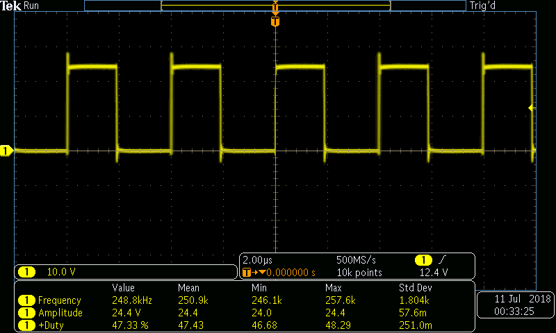
However, I am noticing sever ringing on BOTH the output and input when the FET switches ON and OFF. It's not clear to me if it is a grounding problem or if it's coming off of the regulated 12V. Attached the raw waveform of the BSC340N08NS3GATMA1. The switching frequency is ~250kHz.
We tried an RC snubber between the FET drain and ground, and that only moderately improved. Increasing capacitance on the output and input also slightly improves, but the problem persists.
The biggest problem is that all of the lower voltage regulators (5V and 3.3V) to power the aux chips also see this ringing. As a result we are not able to properly identify lower logic signals (0V) from 3.3V.
Just wondering how to minimize the overshoot/undershoot. Any further information I can provide, please let me know.
Thanks!
Chris