This thread has been locked.

If you have a related question, please click the "Ask a related question" button in the top right corner. The newly created question will be automatically linked to this question.

TPS40211 blows fuse

We have the following circuit

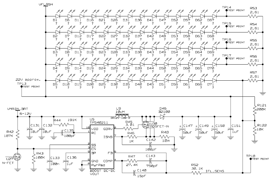
There is one small change to the schematic: R48 (Rsns) was changed to 15mOhm. R121 and R122 are there is case there is no load (LEDs) connected.

For some reason this circuit  keeps blowing a 5A fuse on our board. It works for a few seconds and then blows the fuse.

We looked at the voltage across Rsns ad it is around 50mV while the circuit is working. Then, it goes up to 150mV and then shortly after (within a second) blows the fuse.

Update:

Here is a waveform of the voltages on the MOSFET Gate and across RISND right before the fuse blew.

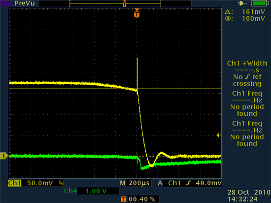
Yellow is V on Rsns and Green is V on the gate of MOSFET.

Why is the circuit blowing the fuse? Is my MOSFET gets stuck on? Why?

  • First, the graphic you included shows a gate voltage of 0V, in this case the MOSFET should be OFF.

    Second, it also shows 170mV as ISNS.  Based on a 15mOhm resistor, that is 11A of current.  11A of current with the gate of the MOSFET 0V strongly suggests the MOSFET has already failed.


    What is the forward voltage of each LED at the 100mA programmed current?

    What is the voltage and currrent rating of the MOSFET?

    You're not using any string current balancing, are you sure the diode voltages are consistant enough to provide string balancing?

    Your control loop also seems very fast (7kHz zero and 300+kHz pole)  I am concerned it's not stable.  Does the switching look stable before the fuse fails?

    It looks like a flash circuit, what turn-on time do you need for the flash?  We might have to slow down the control loop.

  • You are right. We saw that too (MOSFET was on without gate voltage). However, it was not a permanent failure until the 10th power up, when we were trying to measure D-S voltage. The FET was getting too hot. We put a bit of solder flux and the flux started smoking before blowing the fuse. Could that be the result of the unstable control loop?

    We are powering the circuit with a 6.1V source. Our initial thinking was that the G-S voltage was not high enough and was creating a D-S voltage high enough to heat up the chip and cause it to go into constant on state.

    Forward voltage of the LEDs is about 1.5V at 100mA.

    Not sure if the switching was stable though. The switching looked stable for a few seconds. I would like the turn on time to be as fast as possible. How slow would we have to make it?


  • Gennadiy,


    I had a thought.  Boost converters deliver energy during their OFF time, however if their OFF time becomes so narrow that they can't deliver enough energy to the output to maintain the ouptut, the ouptut drops and the control loop demands more current.  This shouldn't look like 0V on the gate drive, but it's still worth checking.


    Make sure the oscilloscope probe is on the MOSFET gate, set to DC coupling and the time scale is 5us / division.  Trigger on rising edge of the MOSFET gate voltage.

    Put a second probe on the COMP pin and a third on the output voltage.  If what I am describing is happening, the duty cycle one the MOSFET gate will be very high (90% duty cycle or higher) and COMP will be well above the ramp peak of 1.8V.  If this is the case, we can increase the minimum off-time by selecting alternate R-C values for the oscillator.

  • Thank you for the response, Peter. We don't have the mosfet to power on today. We hope to get it on Monday.

    However, we had another thought. From previous scope measurements we think we had our Gate voltage less than 4V (maybe around 3-3.5V; unfortunantely we don't have the captures signals to verify yet). At Vgs=4.5 and Id=3A the mosfet (FDS5672 by FairchildSemi) D-S voltage is 0.1V. The datasheet does not show the curve for Vg 3V or 3.5V, however, I would expect Vds to be much higher than 0.1V. Thermal resistance to ambient of the MOSFET is 50 C/W (at 10 seconds) based on the amount of heat produced I would expect the power dissipated to be way over 1W.

    q1: We are powering the circuit with 6V. This reduced the gate drive voltage down from 8V. Is there any information about connecting Vdd to the output to increase the gate drive voltage?

    q2: We desoldered the mosfet (it was bad anyway) and tried powering the circuit without it. We locked at the gate voltage and it was at VDD (which is 6V). However, it was much less (less than 4V) when mosfet was in the circuit. Is it normal for mosfet to pull down the gate drive voltage by more than 2V?


  • q1: We are powering the circuit with 6V. This reduced the gate drive voltage down from 8V. Is there any information about connecting Vdd to the output to increase the gate drive voltage?

    Yes, you can do that and is should work well.  The only restriction is that the input voltage needs to be high enough to meet the UVLO of 4.2V at the VDD pin, so you'll need 4.7-5V for turn-on, depending on the diode forward voltage


    q2: We desoldered the mosfet (it was bad anyway) and tried powering the circuit without it. We locked at the gate voltage and it was at VDD (which is 6V). However, it was much less (less than 4V) when mosfet was in the circuit. Is it normal for mosfet to pull down the gate drive voltage by more than 2V?

    No, that is not considered a normal forward drop on the bypass regulator, however the 28nC gate charge of the FDS5672 MOSFET is drawing 21mA of current through the BP regulator.  The linear regulator was only design to support 15mA of current, so it could be experiencing higher than expected drops.  That MOSFET has an Rdson of 10-14mOhms, depending on the gate drive voltage.  That is extremely low for a FET carrying 1A of current about 65% of the time.

    An Estimate of the expected conduction losses during proper operation come to less than 20mW, but switching losses for 22V @ 1A and 750kHz come to almost 500mW (based on a 30ns rise and fall time on the switching node)  I think you'd find better performance (and possibly lower cost) with a much higher Rdson MOSFET.  Somethign in the 25-50mOhm range.  Just turning the current FET on and off (gate drive losses) is 128mW, much, much higher than conduction losses.


  • Re: first part of response to q2.

    I am confused a bit now. The datasheet says that IGDRV(src,snk) is 400mA typ. Is it something different? I do see why the gate drive would have trouble charging the gate of the mosfet. However, from what I remember the voltage on the gate of the mosfet had some nice (more or less) flat tops which tells me that the gate is charged thus should not be sinking much current.

    Re: second part of response to q2:

    You are right. I am beginning to see the entire picture clearly. We will try to find a better mosfet.

    Are we better off if we reduce the frequency of the regulator by half? This would cut the switching losses in half, right?


  • The pulse current generated by the driver is typically 400mA @ 4V, however the GDRV driver is only designed to support pulses of current.  The average current is provided by the 8V BP regulator, which supports an average current of upto 15mA.  The driver isn't having trouble sourcing 400mA of current to the MOSFET's gate, the BP regulator may be having trouble providing the desired 21mA of average current needed to turn the MOSFET ON and OFF 750,000 times per second.


    Are we better off if we reduce the frequency of the regulator by half? This would cut the switching losses in half, right?

    Yes, that would cut the switching losses in half, and that might be a good first step, but a higher Rdson MOSFET with lower switching charge would still likely offer better efficiency.  Even at half the switching frequency, you'd still have 250mW switching losses and 68mW gate drive losses for a MOSFET to drive 8-10mW conduction losses.  A MOSFET with 2x the Rdson will typically have 1/2 the gate charge.  This would save 125mW switching losses, 34mW of gate drive losses an increase conduction losses only 8-10mW.

  • We will try the following steps:

    1. Use FET with smaller gate charge

    2. Use output to power VDD

    3. Reduce frequency (may consider increasing inductor size if needed).

    As far as the stabilization, we will have to test it once we are able to run the circuit without burning up the MOSFET and blowing the fuse.


  • For stabilization you may want to do your initial testing with a very low bandwidth to eliminate unstable operation as a failure cause. 


    Try changing the 750pF capacitor to 7.5nF, the 15pF capacitor to 150pF and the 27.4k resistor to 2.74k.  This will reduce the gain of the loop by 20dB for stable start-up into a constant load.  Then, once the power stage is working correctly, you can evaluate the control loop to provide the necessary transient response.  If desired, you could even push the loop slower by further decreasing the compesnation loop.  Multiple the capacitor and divide the resistor by the same factor to reduce the gain of the loop by said factor without moving the pole and zero frequencies.

  • We used a different MOSFET and the circuit seems to be working without blowing the fuse. The FET stays warm to the touch and the duty cycle stays unchanged.

    It appears the wrong FET was the problem. The fet selected had a very low RDS-on and high drain current (12A). However, other things were not so good for this application. High gate charge (need higher average current to to charge the gate) loaded the internal BP regulator and resulted in lower voltage on the gate drive pin (not enough voltage on the gate drive pin because BR regulator is overloaded). This in turn combined with higher gate voltage required at ILMAX caused the FET to be not fully turned on thus resulting in higher than normal voltage drop and excessive heat resulting in fail-short condition burning the fuse.

    Thank you.

  • I am very glad we were able to help you.