Other Parts Discussed in Thread: TPS62133
Good morning,
We have made a design with 3x TPS62133A DC/DC converters to generate 3x +5V supply out of +12V,
Everything looks fine and at this moment I am performing some noise and ripple measurements. I noticed that the amount of ripple strongly depends on the load.
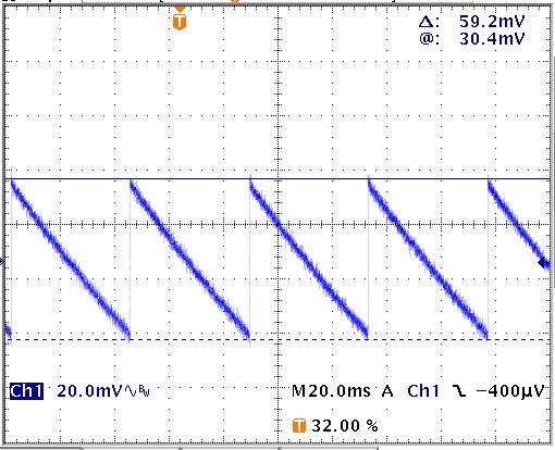
At higher load the ripple is lower compared with light loads or no load. The picture below shows the ripple without a load (this is a +5V supply for external devices). In that case I get a relative high ripple of 59mV at a very low frequency (42 msec). However of course this is not a practical use because normally there will be always a load when using this supply.
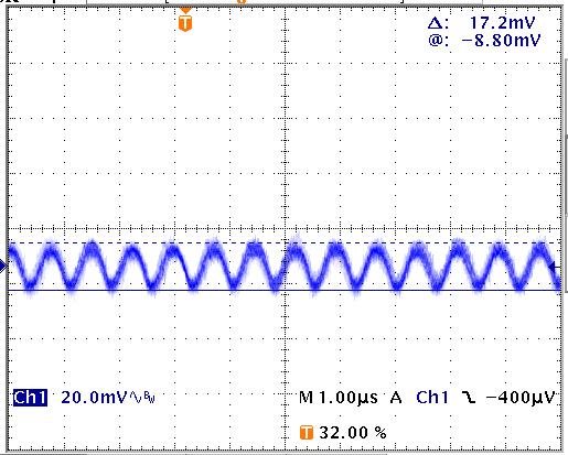
When I put a (resistive) load of 1A the ripple is reduced to 17mV at a frequency around 1.3MHz (I think due to the fact that we connected the FSW input with the voltage output of the converter.
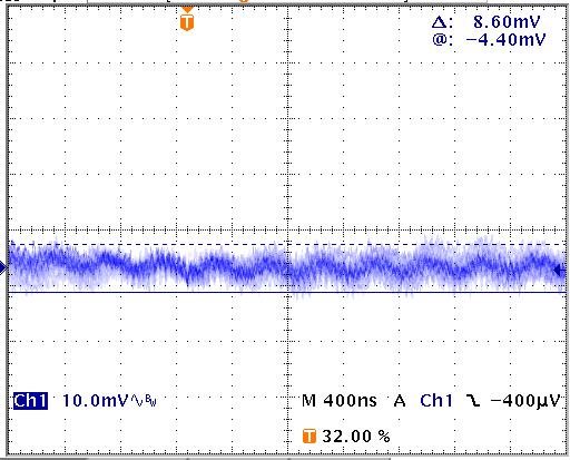
When I measure the ripple at one of the other TPS62133 converters I even measure a very low ripple of less then 10mV (the lowest resolution of my scope) so this looks quite nice.
This is the converter that generates the +5V for all the logic on our PCB,.
So my question is if this looks normal and is it normal that the amount of ripple depends on the load? And is it normal that a relative high ripple a low frequency (first picture) is measured at the output when there is no load at all?
Furthermore the temperature is quite high at 3A load but that is in fact what Webench showed. In normal situations we don't use this maximum load but our customer can connect external devices to this supply until a maximum of 2.5A. I have to make some modifications for our final design (this was just our first proto but it looks quite well) and I was wondering if there are some methods for additional cooling of the device? I have already inserted some thermal via's connected with a large copper ground plane below the device. Maybe I can add some extra copper areas at other layers (we use 6 layers)? I did not find heatsinks for such small devices.
Regards
Chris van der Aar
NTS Systems Development
Eindhoven, The Netherlands


