Other Parts Discussed in Thread: LM25066
Situation is as following, the Overvoltage is set to 13,55V I increase input voltage to 13,6V, the output MOSFET is switched off. Input voltage goes back to 12,5V
Now I am pulling down EN/UVLO pin and VREG for a 100us. And the output FET is not activating. I have designed on my board the reset circuit based on that what stays in the datasheet point:
The SMBus address of the LM25066A is captured based on the states of the ADR0,ADR1, and ADR2pins(GND, NC, VDD) during turnon
and is latched into a volatile register once VDD has exceeded its POR threshold of 2.6 V. Reassigning or postponing the address capture is accomplished
by holding the VREF pin to ground.
Pulling
the VREF
pin low will also
reset
the logic
and erase
the volatile
memory
of the LM25066A.
Once
released,
the VREF
pin will charge
up to its final
value
and the address
will be latched
into a volatile
register
once
the voltage
at the VREF
exceeds
2.4 V.
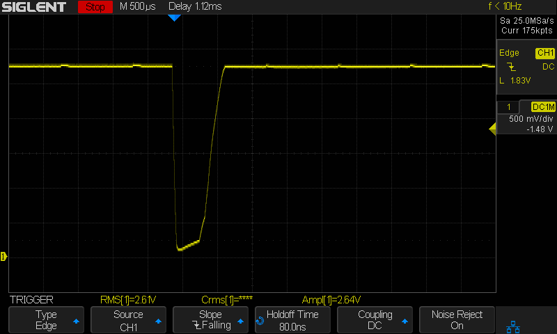
So now after what I see for me the VDD pin should be pulled down not the VREG, maybe VREG only if you need chane or reassign the I2c address. I have looked on the scope at the VREG pin, it was 0,5 V for more than 300us, during the first 100us the Vreg cap is discharging linear down to 0,5V.
Is this a failoure in the datasheet or am I missing something?. Simple, The circuit is no starting on after Overvoltage has occured, even after proper resetting, regarding to the datasheet.