This thread has been locked.

If you have a related question, please click the "Ask a related question" button in the top right corner. The newly created question will be automatically linked to this question.

LM3150: Minimum off-time

Part Number: LM3150
Other Parts Discussed in Thread: CSD18543Q3A,

Hi,

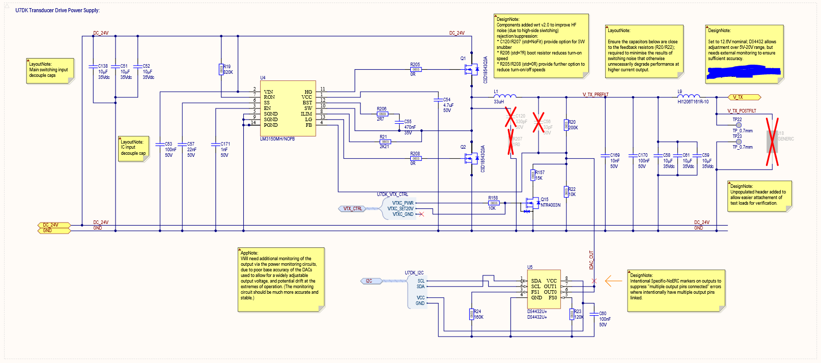
In section 9.2.2.3 of the LM3150 data sheet in the "Determine Ron and fs" section it states that an extra 200ns is added as headroom for the turn on / off delay of the external MOSFET. If we use MOSFETs with much lower turn on / off delays for example (CSD18543Q3A) which have specified turn on / off of 9/8ns can we use (toff-min + 10ns) instead of (toff-min + 200ns)?

  • Hello Oliver,

    I suggest keeping the 200ns delay as it is not only referring to the slew rates of the FETs turning on/off, but it is also taking into account the delays associated with the internal circuitry which include PWM propagation delays etc....

    Hope this helps?

    David.
  • Hello David,

    Thanks for the quick response, that is helpful, I've made some PCBs that have a measured Toff of <300ns and I haven't measured or observed any issues. What failure mode could I expect when the Toff is too low? I thought that the bootstrap cap may discharge too much given the lower recharge time possibly causing the high side Vgs too become too low, I've inspected the PCB and haven't observed this though.

    The load current and output capacitance has a large potential range depending on another PCB that is connected to the regulator output. (30uF @ <10mA up to 2.5mF @ 3.0A). This output range requirement has resulted in a high(er) switching frequency and therefore lower Toff times.

    Many Thanks,

    Oliver

  • Hello Oliver,

    You are right, smaller Toff times give less times for Cboot to recharge.  should this occur, you will get erratic switching behavior.  Another potential issue is poor load and line transient responses when violating Toff min times.  This is because the Duty cycle is saturated and can not increase duty cycle further should the load increase suddenly, or vin dip slightly further to a lower point.

    Hope this helps?

    David.

  • Hi David,

    That is useful information thanks, I've been seeing some failures of the regulator on multiple PCBs (~33%), sometimes resulting in the destruction of the high side MOSFET, othertimes causing an output voltage of <3V when the feedback resistors have been chosen to output 20.4V. I can provide the schematic next week if this would help, but for now I've attached a scope screenshot of the SS pin. This is the typical waveform seen when the device is outputting <3V but not having killed either of the switches. Looking at the block diagram in the datasheet, I believe this SS waveform should occur if the VCC UVLO, Thermal shutdown or EN pin have triggered. None of these should have triggered on this particular PCB as the EN and VCC pins measure correct values and the package is not close to the thermal shutdown temperature.

    Do you know any other causes of this? Any help would be greatly appreciated. FYI the MOSFETs are both TI CSD18543Q3A devices.

    Many Thanks,

    Oliver

  • Hello Oliver,

    Short Circuit protection also pulls on the SS pin.

    Please can you post schematic and also your PCB Layout?

    Thanks.

    David.
  • Hello David,

    U5 is a current DAC that isn't used at preset, it's output leakage current is +-1uA when programmed for zero current.

    Topside PCB layout:

    Bottom side PCB layout:

    Many Thanks,

    Oliver

  • Thanks for sharing the schematic Oliver,

    I think the layout may have something to do with your failure issue.  2 layer boards are a little more difficult to do than 4 and can give rise to cross conduction of the MOSFETs if the PGnd is not tied back to the low side FET with a low impedance path.

    Please see below suggest floor plan.  Suggest you hack the board to suit and retest.

    Hope this helps?

    David

  • Hi David,

    Thanks for the advice, I should have said in my last message, the PCB is actually a 10 layer board, I just removed the inner planes/layers for convenience. There is a pretty tight loop from the lowside FET back to PG using inner ground plane, there's 8 vias at the FET ground and 9 vias close to Pgnd where the thermal pad is. I can see how this could be improve though, I'll give it a try.

    I've made some more progress today in tracking down the problem. It seems that all of the PCBs I've tested so far that have poor regulator behaviour are highly temperature dependant. They take a while to reach the desired output voltage (~10 seconds) when powered on from cold. Using freezer spray to cool the LM3150 down causes the output voltage to drop and regulate very poorly until the part returns to its "normal" operating temperature. On the PCBs that work fine this is not the case, they continue to regulate well regardless of operating temperature as expected.

    There only seems to be a single batch that we've had produced that have this temperature dependence, two other batches produced have all worked correctly. One of the LM3150 codes from the poor batch of PCBs is 79AXE0U. Again, many thanks for the help with this.

    Oliver
  • Hello Oliver,

    Sometimes when customers see an issue with a lot they believe that the issue is with our manufacturing. The reality is often that an application issues is uncovering a variation in our process, unfortunately for the customer the issue is not that we are outside the limits we guarantee, but an application does not work within our guaranteed limits.

    Hitting the device with freeze spray is a little aggressive if the nozzle is too close to the package and blasted onto the pins, this can cause moisture and depending on the impurities on the board can introduce issues due to significant impedance shifts not realized in the true application. With that said, the fact that you have some parts working and some that do not, is likely due to the fact that the existing design is marginal for some reason? 

    There are two items that can cause output voltage to lose regulation.

    1. Ilimit issue
    2. Feedback issues

    The fact that the SS is pulling low suggests to me that the device is hitting current limit for some reason.


    Perhaps the issue is partial cross conduction of the HSF and LSF? A quick fix/experiment is to just place a 10 ohm resistor in the HSF gate slowing down the DV/DT on the Switch node and see if the issue goes away?

    Hope this helps?

    David.

  • Hi David,

    Apologies I wasn't trying to point the finger, I was more suggesting that there may have been some poor handling of the parts during or before assembly and/or just poor PCB assembly for this poor batch. I agree that this is much more likely to be the application not working within the process variation of the part.

    I've just checked to SS pin on one of the parts that was poor at low temperatures, it is not pulling low now. It is staying at ~0.6V even when the regulation is very poor. I'll see if I can slow down the HSF and see if the issue goes away as you've suggested.

    Many Thanks,
    Oliver
  • Hello Oliver,

    No need to apologize, I was not trying to apportion blame, just informing :).

    Let me know how the tests go...

    Thanks.

    David.

  • Hi David,

    I've added a 10 ohm resistor to the HSF, I've also included a diode in parallel with the resistor that will be forward biased on the falling edge to attempt to avoid both FETs conducting on either switching edge.

    The attached screenshot shows both FET gates waveforms with this modification. The PCB is still regulating poorly when the temperature changes. I will keep the mods in place for now to rule out the cross conduction problem. Where would you advise looking next? I guess the feedback is potentially unstable due to large output capacitance and low ESR. I could try the feedforward network that is currently not fitted?

    Thanks,

    Oliver

  • Hello Oliver,

    Thanks for sharing your waveforms. Can you zoom into the point that the HSF pulls high and make the LSF GD scope capture 1V/div?

    Thanks.

    David.

  • Hello David,

    I have zoomed in to the rising edge of the HSF gate:

    I've done a better job of grounding the LSF probe so some of the ringing has been removed. Here is a screenshot of the HSF switching off FYI:

    Thanks,

    Oliver

  • I should have also mentioned, the screenshots above are from a different PCB that does not have the 10ohm gate resistor mod or diode. The modded PCB is now in the mode where the SS pin pulling low and therefore not regulating.
  • Hello Oliver,


    Are you measuring right at the Gate and source of each FET? if not please do so.

    Looking at the falling edge, it looks like there may be partial cross conduction? Can you place a Diode (Say BAT54) across the 10ohm. Cathode to Lo and Anode to Gate of FET. We need the HSF GD to snap off quickly before the LSF GD comes up. Can you please remeasure.


    Thanks.

    David.