Other Parts Discussed in Thread: TPS2511
Tool/software: WEBENCH® Design Tools
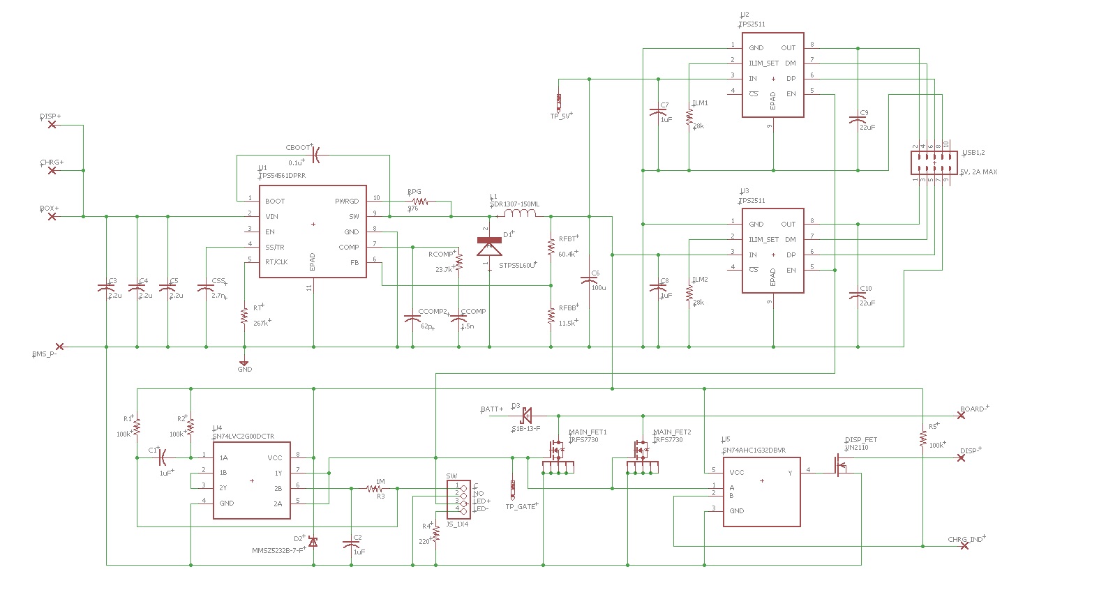
I used WEBENCH to generate a design for the buck converter TPS54561DPRR chip, the full schematic for my design is attached below. There were two deviations I made in my schematic from the WEBENCH design, that is the diode on the output, STPS5L60U, and the inductor, SDR1307-150ML. For the diode, instead of it handling 20A, it only handles 5A max, I decided this because I am only going to be drawing 4A total on my USB ports, and way less than 1 amp for the other loads in the circuit. As for the inductor, I stuck with a 150ML version instead of the 100ML suggested by the WEBENCH design, because I already had them purchased, they had the same footprint, and I figured they were compatible enough that it wouldn't make a difference.
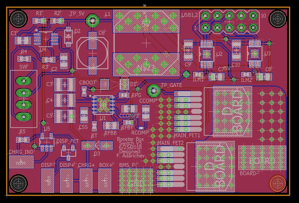
The issue is that I've assembled 3 copies of this PCB, and I'm still having issues, and I want to make sure it is not something in the design which I am not understanding. That being said, one of these boards did 100% function exactly as intended, but did not continue working the next day when I tried testing again.
Here is a list of the issues that I am seeing:
- When I connect a 37V lipo battery pack to BOX+ and BMS_P- terminals (the input of the buck converter), the trace pops at the input pin of the buck converter, so the trace just detaches from the board and the buck converter chip is fried. This would lead me to believe there is some sort of inrush current problem?
- With a probe at TP_5V, the output of the buck converter at the bulk output capacitor, it fluctuates between 2.2-3.3 V, so the output is unstable, so after damaging it, it does not behave as intended, although it is not shorted?
- There is a short between the output of the buck converter and ground, after being fully damaged, but with no popping of a trace?
- When the output of the buck converter is a stable 5V as intended, the output of the TPS2511 USB regulators does not sustain 5V, so the loads that I put on them (USB bike lights that draw 1.6A max), do not turn on. This is a separate issue from the buck converter as I see it, but maybe the buck converter current output is a problem?
- When the output of the buck converter is a stable 5V as intended, the SN74LVC NAND gates do not switch the USB regulators, and the switch LED does not light up. WHen this happens, I am also seeing a short from TP_GATE+ to ground, so that would indicate a fried NAND chip, so I have tried replacing those too, also with no change.
In summary, I'm seeing very inconsistent results, and I am confident with my pick+place, reflow, and testing set up process. I used all fresh components on one of the boards and it didn't work. But, I used some older components on the board that did actually work. I solder things with an iron and a hot air gun, usually at 300 degree Celsius, but sometimes at 350 degrees Celsius, but I have not had problems with overheating and damaging components like this in the past.
Thanks for the help!