This thread has been locked.

If you have a related question, please click the "Ask a related question" button in the top right corner. The newly created question will be automatically linked to this question.

TPS56121: tps56121_1

Part Number: TPS56121

Hi, buddy:

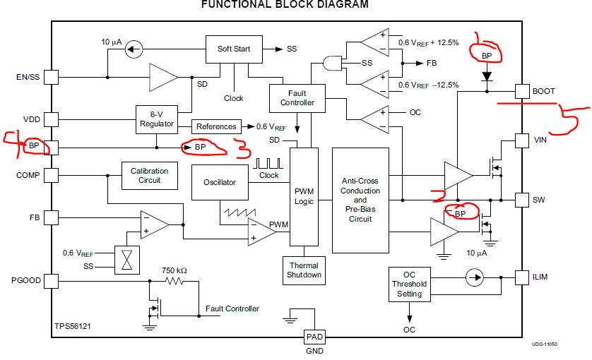
    I have 2 question about TPS56121 ,

    1: what's the four BP means, and what's the function of them in particular situation?

    2: how does the bootstrap works?  Vbp = ?  and is the Vbp conneted to Pin BOOT, and then is bootstrap the SW, or SW bootstrap the pin BOOT through an external capacitor C14(100nF) ?

  • Hello Xiaopan,
    1. The BP is an output of LDO from VDD. In general, any IC needs a voltage to bias the internal logic/circuit such as reference voltage and uses to drive the power MOSFETs (1 and 2 marks on the block diagram). The LDO needs output capacitor (mark #4) to stable LDO and deliver fast di/dt to the internal logic (mark #3).
    2. The boot capacitor: there are many documents available to describe how it functions. Please see this link below as an example. In general, the charge in the boot capacitor uses to charge the gate voltage of upper mosfet at beginning of its on-time. To recharge this boot capacitor during off-time, BP (mark #1) charges to this boot capacitor through the diode.
    www.ti.com/.../slva444.pdf
    Kit
  • Hi Xiaopan,
    1. Also, please see the datasheet page #3 which has the description of BP pin.
    Kit